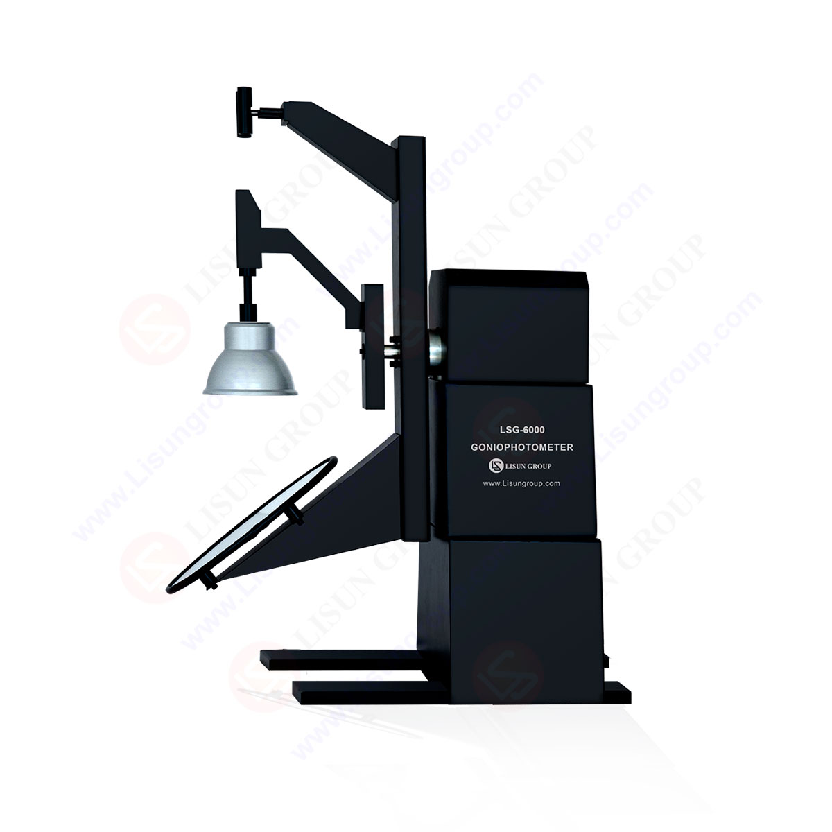
LM-79 Moving Detector Goniophotometer (Mirror Type C)
LSG-6000
High Precision Rotation Luminaire Goniophotometer
LSG-1890B
High Precision Rotation Luminaire Goniospectroradiometer
LSG-1890BCCD
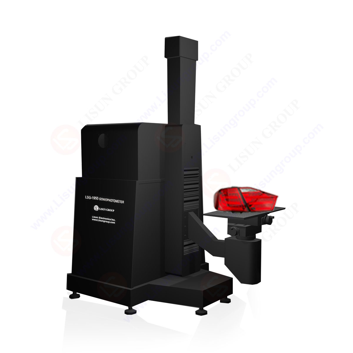
Goniophotometer for Automotive and Signal Lamps
LSG-1950
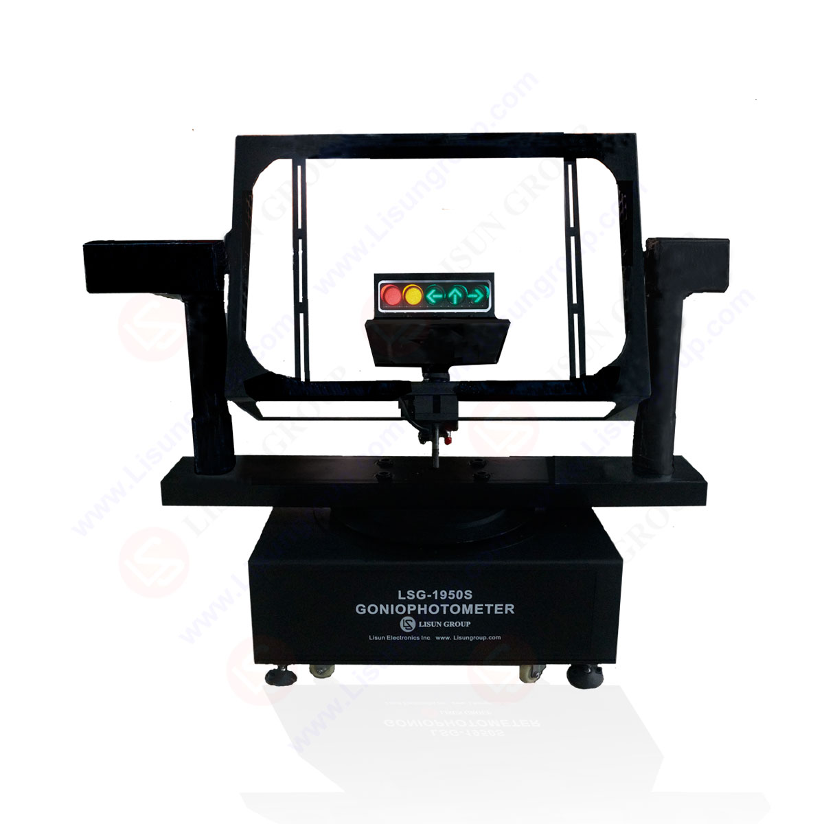
Goniophotometer for Traffic Signal Lamps
LSG-1950S
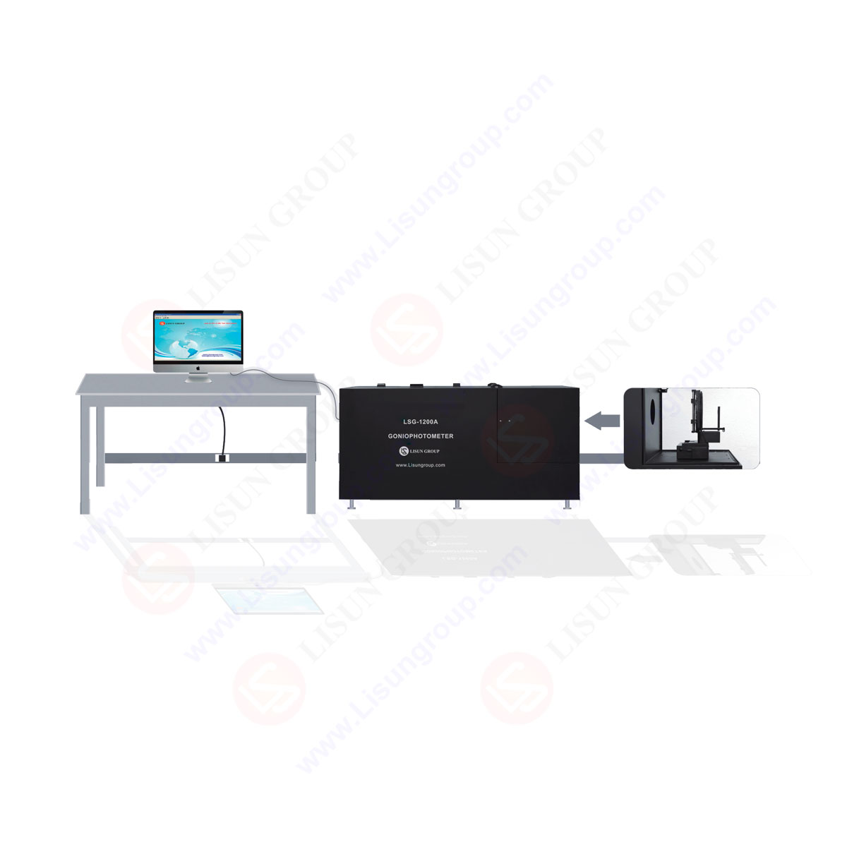
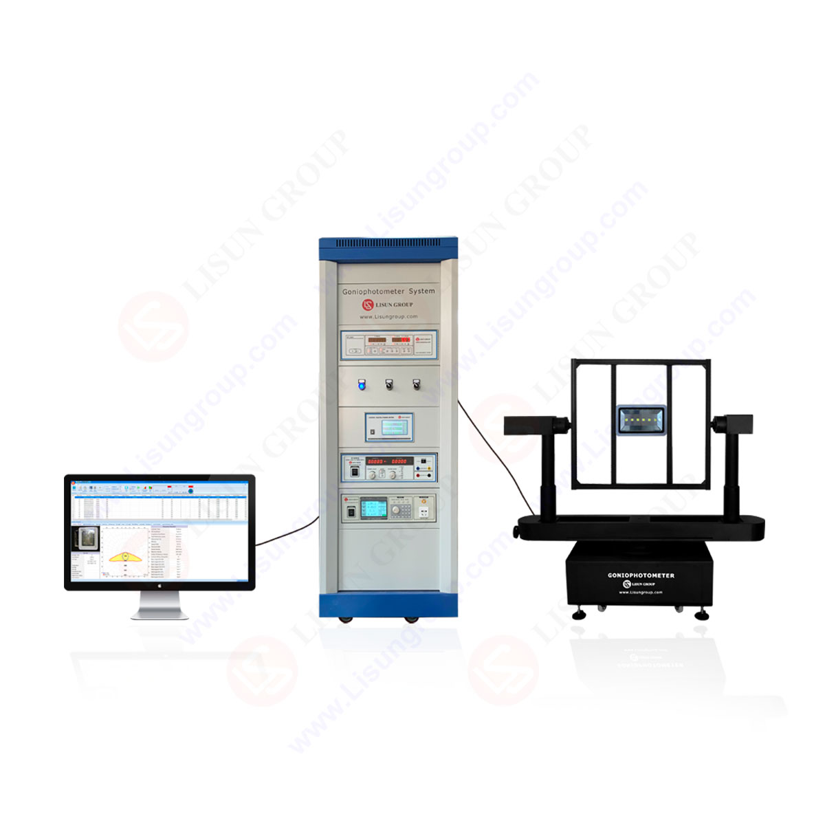
Compact Goniophotometer
LSG-1200A

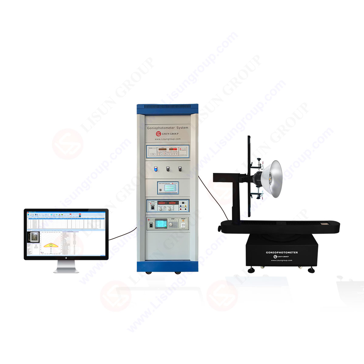
Near Field Moving Detector Goniophotometer
LSG-1900B
Select an organization
to browse standards
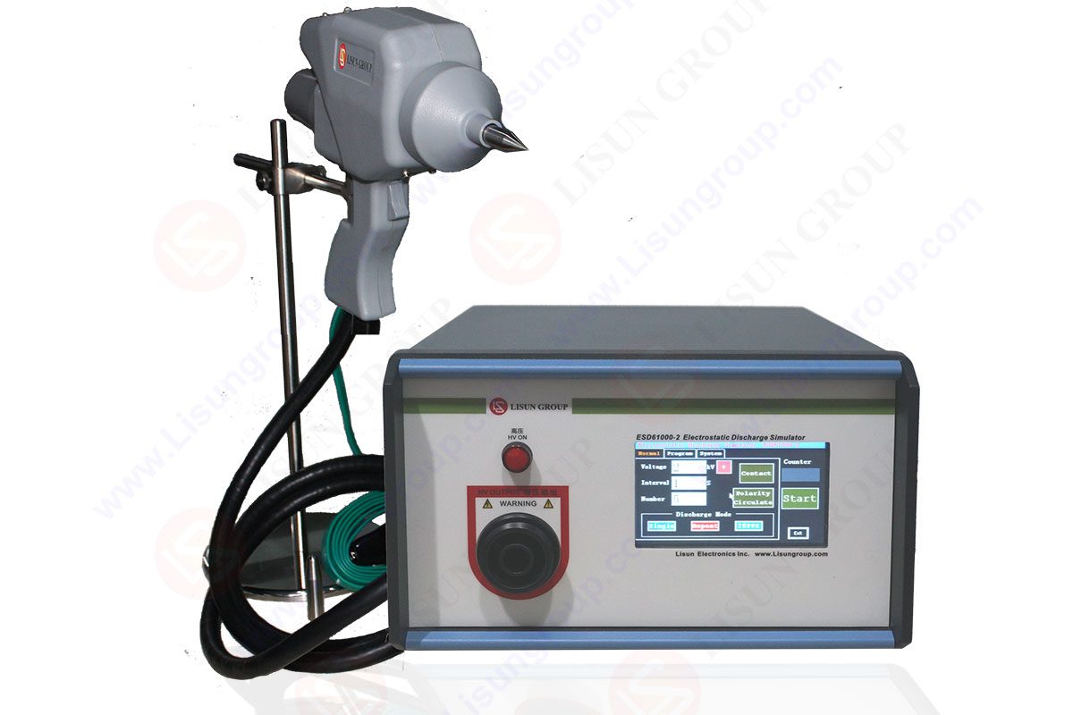
ESD simulator
An ESD simulator, often known as an ESD gun, is a portable device that is used to evaluate the resistance of devices to electrostatic discharge (ESD). These simulators are used in laboratories that specialize on electromagnetic compatibility (EMC). ESD pulses are high-voltage pulses produced when two items with opposing electrical charges come into contact. They can be recreated in a test environment to ensure that the gadget under test is resistant to static electricity discharges.

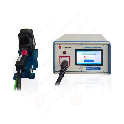
ESD61000-2_Electrostatic Discharge Simulator
ESD testing
ESD testing is required for most vendors of automotive components as part of the obligatory electromagnetic compatibility testing. It is frequently beneficial to automate these tests to eliminate the human factor. ESD testing is required for most vendors of automotive components as part of the obligatory electromagnetic compatibility testing. It is frequently beneficial to automate these tests to eliminate the human factor.
Types of an ESD IC tester
Logic testers, memory testers, and analogue testers are the three types of testers. Normally, IC testing is done in two stages: wafer testing (also known as die sorting or probe testing) and package testing (also known as final testing) after packing. Wafer testing employs a prober and a probe card, whereas package testing employs a handler, a test socket, and a tester.
ICs
Linear integrated circuits (ICs) such as op amps, in-amps, and data converters are protected before they are put on a printed circuit board. That is an out-of-circuit condition. In such a state, ICs are fully at the mercy of their surroundings in terms of any stressful voltage surges they may encounter. Electrostatic discharge, or ESD as it is more frequently known, causes the majority of the dangerous voltage surges. This is a single, quick, high current electrostatic charge transfer caused by one of two scenarios.
These conditions are
1. Transfer of direct contact between two objects with different potentials (sometimes called contact discharge)
2. When two items are in proximity, they generate a strong electrostatic field (sometimes called air discharge) The primary sources of static electricity are largely insulators and are often synthetic materials, such as vinyl or plastic work surfaces, insulated shoes, finished wood chairs, scotch tape, bubble pack, soldering irons with ungrounded tips, and so on.
Because their charge is not easily spread over their surfaces or transferred to other objects, the voltage levels created by these sources can be exceedingly high. The triboelectric effect is the creation of static electricity induced by rubbing two substances together.
• Walking on a Carpet 1000V – 1500V
• Walking on a Vinyl Floor 150V – 250V
• Managing Material Protected by Clear Plastic Covers 400V – 600V
• Handling Polyethylene Bags 1000V – 2000V
• Polyurethane Foam Poured into a container 1200V – 1500V
Note: The above assumes a relative humidity of 60%. Voltages can be more than ten times higher with low RH (30%).
ESD’s high voltages and high peak currents can destroy integrated circuits. Precision analogue circuits, which frequently have very low bias currents, are more vulnerable to damage than conventional digital circuits because traditional ESD-protection architectures increase input leakage and hence cannot be employed.
The most common manifestation of ESD damage for the design engineer or technician is a catastrophic failure of the IC. ESD exposure, on the other hand, might cause increased leakage or deterioration of other features. If a device does not appear to satisfy a data sheet standard during examination, ESD damage should be evaluated. Outlines some important elements about ESD-induced failures.
ESD Failure Mechanisms
• Dielectric or junction damage
• Surface charge accumulation
• Conductor fusing ESD
Damage Can Cause
• Increased leakage
• Degradation in performance
• Functional failures of ICs
ESD Damage is often Cumulative; for example, each ESD “zap” may cause more junction damage, eventually causing the device to fail.
ESD protection
Understanding ESD harm Protective packaging is used for all ESD-sensitive equipment. ICs are typically packaged in conductive foam or antistatic shipping tubes, which are subsequently sealed in a static dissipative plastic bag. The sealed bag is labelled with a unique code that describes the proper handling instructions.
The presence of outside packaging notices alerts the user that device handling practices suitable for ESD protection are required. Furthermore, data sheets for ESD-sensitive ICs usually include a prominent declaration to that effect. All static sensitive gadgets are individually packaged in protective packaging and labelled with handling instructions.
Electrostatic charges as high as 4000 V can easily develop on the human body and test equipment and discharge undetected. Although the ADXXX includes patented ESD safety circuitry, electronics subjected to high energy electrostatic discharges may sustain irreparable damage. To avoid performance deterioration or loss of functionality, adequate ESD safeguards are recommended. Protection is relatively simple once ESD-sensitive devices are recognized.

ESD-883D
Electrostatic Discharge (ESD) IC Tester
Keeping integrated circuits in their original protective packaging is obviously a first step. Discharging potentially dangerous ESD sources before IC damage occurs is a second stage. Such voltages can be discharged fast and safely using a high impedance. A workbench with a static-dissipative surface is a critical component for ESD-safe IC handling. A 1 M resistor connects the surface to ground, dissipating any static charge while protecting the user from electrical ground fault shock dangers. If the bench tops are nonconductive, a static-dissipative mat should be installed in addition to the discharge resistor.
Remember that if a charged IC is discharged through a low impedance, a high peak current may flow. This is exactly what happens when a charged IC comes into touch with a grounded copper covered board. When the same charged integrated circuit is placed on a high impedance surface. The peak current, however, is insufficient to destroy the equipment.
A variety of staff handling strategies are essential for minimizing ESD-related harm. When handling ESD-sensitive electronics at the workstation, a conductive wrist strap is recommended. The wrist strap prevents typical operations like stripping tape from parcels from causing IC damage. Again, a 1 M resistor is required from the wrist strap to the ground for safety. When assembling PC boards with ESD-sensitive ICs, all passive components should be placed and soldered before the ICs. This reduces the sensitive electronics’ ESD exposure. Of course, the soldering iron must have a grounded tip.
ESD protection for integrated circuits necessitates the involvement of both the IC producer and the customer. IC makers have a vested interest in delivering their devices with the best level of ESD protection feasible. IC circuit designers, process engineers, packaging specialists, and others are continuously on the lookout for new and improved circuit designs, processes, and packaging solutions that can withstand or shunt ESD energy.
A comprehensive ESD protection strategy, on the other hand, necessitates more than just incorporating ESD protection into ICs. Users of integrated circuits must also give their staff with the appropriate knowledge and training in ESD handling techniques, so that protection may be built in at all critical stages along the process. Outlined as follows.
Analog devices
• Circuit Design and Fabrication
• Create products with the highest level of ESD protection while maintaining essential analogue and digital performance.
• Pack and Ship
• Static dissipative material should be packed in. Packages should be labelled with an ESD warning.
Customers
• Incoming Inspection
• Inspect at grounded workstation. Minimize handling.
• Inventory Control
• Store in original ESD-safe packaging. Minimize handling.
• Manufacturing
• Deliver to work area in original ESD-safe packaging. Open packages only at grounded workstation. Package subassemblies in static dissipative packaging.
• Pack and Ship
• Pack in static dissipative material if required. Replacement or optional boards may require special attention.
ESD Protection necessitates a partnership between ADI and the end user, including control at key points. When breadboarding and assessing ICs, extreme caution should be exercised. Because the consequences of ESD damage can be cumulative, persistent misuse of a device can lead to failure. Inserting and removing ICs from test sockets, storing devices for evaluation, and adding and removing external components from the breadboard should all be done with correct ESD safeguards in mind. If a device fails during the development of a prototype system, repetitive ESD stress may be the cause.
The key word to remember with respect to ESD is prevention. ESD damage cannot be undone, nor its effects can be compensated.
ESD IC models and testing
Some applications are more susceptible to ESD than others. ICs situated on a PC board surrounded by other circuits are far less sensitive to ESD damage than circuits that must interface with other PC boards or the outside world. These ICs are not typically specified or guaranteed to meet any specific ESD criteria (except for classified devices). The RS-232 interface port ICs on a computer are a good example of an ESD-sensitive interface since they are easily exposed to high voltages.
The test techniques and restrictions must be established to ensure ESD performance for such devices. To assess the vulnerability of devices to ESD, a plethora of test waveforms and requirements have been established. The Human Body Model (HBM), the Machine Model (MM), and the Charged Device Model are the three most prominent waveforms now in use for semiconductor or discrete devices (CDM).
Because each of these models depicts a fundamentally different ESD event, there is little consistency between the test findings for these models. Since 1996, all electronic equipment delivered to or inside the European Community has been required to fulfil Electromechanical Compatibility (EMC) norms stated in IEC1000-4-x regulation.
It should be noted that this does not apply to individual ICs, but rather to the whole product. These standards, as well as test techniques, are defined in the different IEC1000 specifications. IEC1000-4-2 requires compliance testing to be performed using one of two coupling methods: contact discharge or air-gap discharge. A direct connection to the unit being tested is required for contact discharge.
Airgap discharge employs a larger test voltage but avoids direct contact with the unit being tested. The discharge pistol is advanced toward the equipment being tested, creating an arc across the air gap, hence the phrase air discharge. The humidity, temperature, barometric pressure, distance, and rate of closure of the discharge gun all have an impact on this procedure. While less realistic, the contact discharge method is more repeatable and is gaining favor over the air-gap method.
ESD generator
The test generator mimics electrostatic discharge in accordance with IEC / EN 61000-4-2. For laboratory tests, rely on the Equipment Under Test (EUT) and the test setup. The IEC standard specifies two testing methods:
1. Discharge of air the test generator must be relocated to the EUT using this manner. The high voltage discharge is in the air. The test voltage can be adjusted up to 30kV. Each single pulse’s very short rising time generates a large RF spectrum and interference.
2. Discharge through contact The EUT is attached to the discharge electrode with a sharp tip. A vacuum relay serves as the discharge switch.
FAQs
What is an ESD tester?
Electromagnetic compatibility testing is known as ESD testing (EMC test). ESD testing replicates numerous electrostatic effects that equipment may encounter either in transit or in operation. An electrostatic discharge test examines whether a product’s ESD protection area and procedures are followed.

What is electrostatic discharge in IC?
A charged object touching an IC, a charged IC hitting a grounded surface, a charged machine touching an IC, or an electrostatic field creating a voltage strong enough to rupture a dielectric can all cause ESD.
Lisun Instruments Limited was found by LISUN GROUP in 2003. LISUN quality system has been strictly certified by ISO9001:2015. As a CIE Membership, LISUN products are designed based on CIE, IEC and other international or national standards. All products passed CE certificate and authenticated by the third party lab.
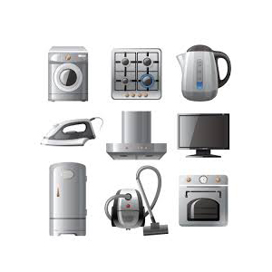
Our main products are Goniophotometer, Integrating Sphere, Spectroradiometer, Surge Generator, ESD Simulator Guns, EMI Receiver, EMC Test Equipment, Electrical Safety Tester, Environmental Chamber, Temperature Chamber, Climate Chamber, Thermal Chamber, Salt Spray Test, Dust Test Chamber, Waterproof Test, RoHS Test (EDXRF), Glow Wire Test and Needle Flame Test.
Please feel free to contact us if you need any support.
Tech Dep: Service@Lisungroup.com , Cell/WhatsApp:+8615317907381
Sales Dep: Sales@Lisungroup.com , Cell/WhatsApp:+8618117273997

LISUN’s Motor-Operated Tool | Power Tool Testing solutions strictly comply with a range of core international standards, providing full support for safety and electromagnetic compatibility (EMC)...

LISUN’s electric toy testing solutions cover IEC 62115, EN 71-1, ASTM F963 standards. Including electrical, mechanical, flammability tests to ensure toy safety compliance globally.
LISUN’s transformer test solutions meet IEC 61558-1, IEC 60076-1, IEC 62041 standards. Covering safety, performance, EMC tests, ensuring transformers comply with global requirements.

LISUN’s energy meter testing solutions align with IEC 62052-11, IEC 62053 series standards. Covering safety, electrical, environmental, and EMC tests, we help manufacturers meet global compliance...
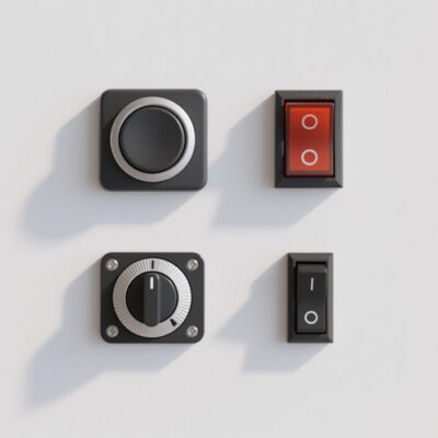
LISUN’s household and appliance switch testing solutions meet IEC 60669, IEC 61058, IEC 62271 standards. Covering electrical, mechanical & EMC tests for global compliance.

LISUN’s automotive electronics test solutions cover photometric/colorimetric testing, EMC immunity tests, IP waterproof/dustproof tests, and environmental simulation, meeting ISO, SAE, ECE standards.
LISUN has all equipment according to the IEC60669 measurement, including environmental chamber, IP code waterproof dustproof test, switch lift test, etc.

Lisun can supply full test solutions for fluorescent lamp, including integrating sphere system, goniophotometer system, EMI EMC test, electronic ballast tester, electrical safety test, etc.

For the CFL design and manufactory, LISUN can supply a full quality control test solution, including photometric, colorimetric, electricity, flicker, IES candela distribution, surge test, electrical...

LISUN’s LED driver test solutions cover lab testing, online testing, EMC/EMI tests, and safety checks, meeting IEC 60335, UL 60335 standards for reliable performance evaluation.

 中文简体
中文简体