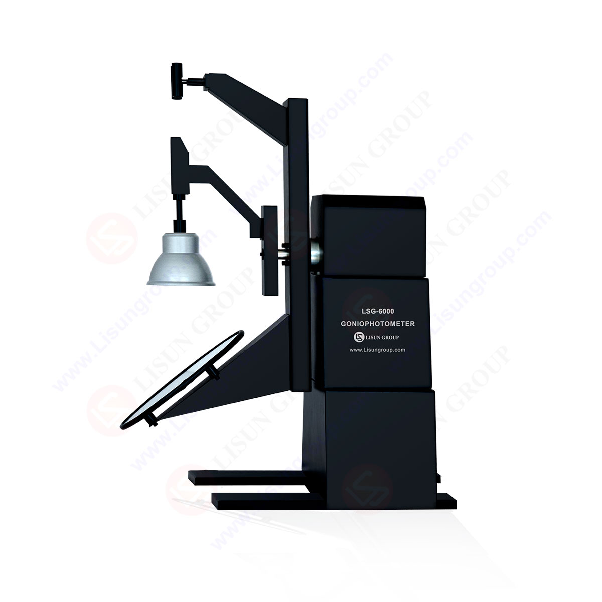
LM-79 Moving Detector Goniophotometer (Mirror Type C)
LSG-6000
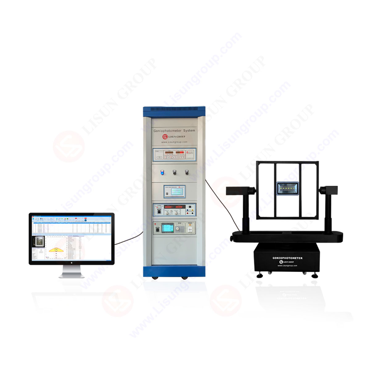
High Precision Rotation Luminaire Goniophotometer
LSG-1890B
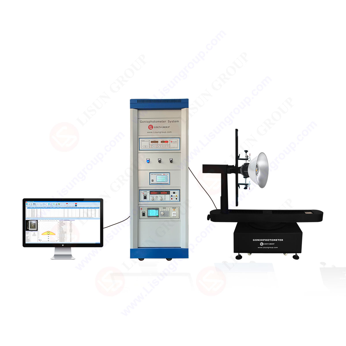
High Precision Rotation Luminaire Goniospectroradiometer
LSG-1890BCCD
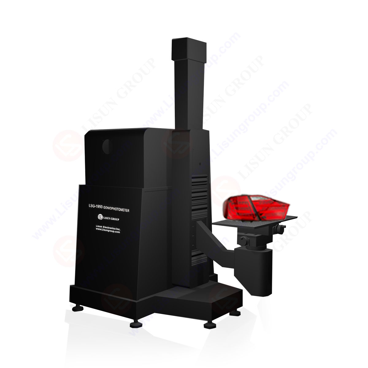
Goniophotometer for Automotive and Signal Lamps
LSG-1950
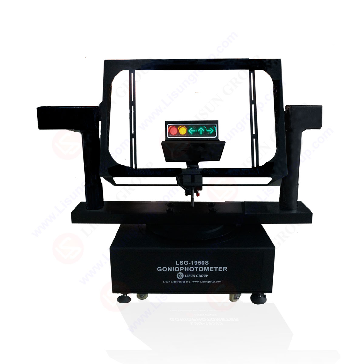
Goniophotometer for Traffic Signal Lamps
LSG-1950S
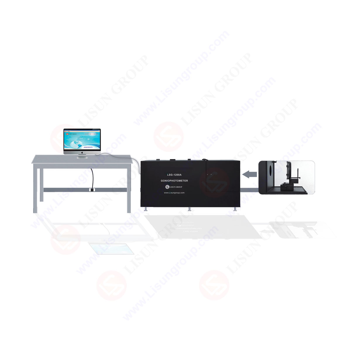
Compact Goniophotometer
LSG-1200A

Near Field Moving Detector Goniophotometer
LSG-1900B
Select an organization
to browse standards
In addition to the selection and circuit design of components, good printing circuit board (PCB) design is also a very important factor in electromagnetic compatibility. The key to the design of PCB in EMC is to reduce the return area as much as possible and let the return path flow in the direction of the design. The most common return current comes from the cracks of the reference plane, the transformation of the reference plane layer, and the signal flowing through the connector. Clash capacitors or decoupling electric containers may solve some problems, but it is necessary to consider the overall impedance of capacitors, perforated, pads and wiring.
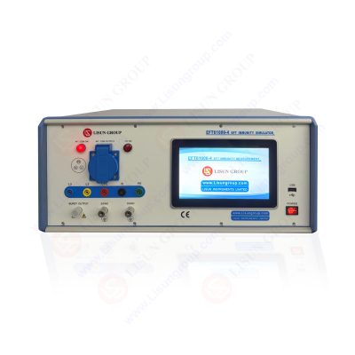
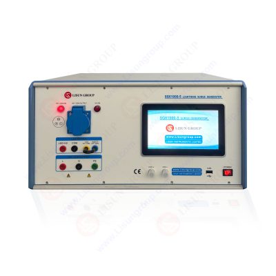
LISUN SG61000-5 fully automatic surge generator (also called lightning surge immunity test, combination wave generator, surge current generator/surge voltage generator, combined surge voltage and current generator) . LISUN surge generator and other EMC test instrument design with PCB board. If meet any problem, only need to replace the PCB board.

surge generator
PCB layered strategy
The thickness of the thickness, the perforated process and the number of layers of the circuit board in the circuit board design are not the key to solving the problem. The excellent layered stack is the bypass and decoupling of the power supply flow. The key to blocking the electromagnetic field of the signal and power supply. From the perspective of the signal line, a good layered strategy should be to put all signal wiring on one or several layers, these layers are next to the power layer or ground layer. For the power supply, a good layered strategy should be adjacent to the power layer and the ground layer, and the distance between the power layer and the ground layer as small as possible. This is what we say “layered” strategy. Below we will talk about excellent PCB stratification strategies.
1. The projection plane of the wiring layer should be in its return plane area. If the wiring layer is not in the projection area of its return plane layer, there will be signal lines outside the projection area during the wiring, which will cause the “edge radiation” problem, and it will also cause the signal loop area Essence
2. Try to avoid adjacent settings of the wiring layer. Because the parallel signal line on the adjacent wiring layer will cause signal strings, if the wiring layer is not adjacent to, the distance between the layer between the two wiring layers should be appropriately pulled to reduce the layer spacing between the wiring layer and its signal loop.
3. The adjacent plane layer should avoid its projection plane overlap. Because when the projection overlaps, the coupling capacitance between the layers will cause the noise between the layers to couple.
Multi -layer board design:
When the clock frequency exceeds 5MHz, or the signal rising time is less than 5ns, in order to make the signal loop area be well controlled, multi -layer board design is generally required. Pay attention to the following principles when designing a multi -layer board:
1. Key wiring layers (clock lines, bus, interface signal line, radio frequency cable, reset signal line, chip signal line, and various control signal cables, etc.) should be adjacent to the complete ground plane. The signal line is generally a signal line with strong radiation or extremely sensitive. Near the ground surface wiring can reduce its signal loop area, reduce its radiation intensity or improve the anti -interference ability.
2. The power supply plane should be compared to its adjacent plane internal shrinkage (the recommended value is 5h to 20h). Compared with its reflux ground surface shrinkage, the power plane can effectively inhibit the “edge radiation” problem, as shown in the figure below.

Power plane should be contracted from its adjacent ground plane
In addition, the single -board owner’s working power plane (the most widely used power supply plane) should be adjacent to its ground plane to effectively reduce the circuit area of the power current.
3. Whether the single board TOP and BOTTOM layers have no signal lines ≥50MHz. If so, it is best to take the high -frequency signal between the two plane layers to inhibit its radiation of space.
Single -layer board and double -layer board design:
For the design of single -layer and double -layer boards, the design of key signal lines and power cords should be paid mainly. There must be a ground line near the power supply line to reduce the area of the power current circuit.
The two sides of the key signal line of the single -layer board should be “Guide Group Line”, as shown in Figure below. There should be a large area pavement on the projection plane of the key signal line of the double -layer board, or the same -layer plate processing method, and the “Guide Group Line” should be designed, as shown in the figure. On the one hand on both sides of the key signal line, the signal area can be reduced on the one hand. In addition, it can also prevent string disturbance between the signal line and other signal cables.

Guide Ground Line
Note: The red line is the key signal line, and the blue line is the ground line
PCB layout skills
When designing the PCB layout, the design principles of the straight lines along the signal flow to the straight line should be fully surrounded as much as possible. This can avoid direct coupling of the signal and affect the signal quality. In addition, in order to prevent interference and coupling between the circuit and the electronic components, the placement of the circuit and the layout of the component should be followed as follows:
1. If the interface is “clean” on the single board, the filter and isolation device should be placed on the isolation band between the “clean” and the place of work. This can avoid filtering or isolation devices coupled to each other through the plane layer to weaken the effect. In addition, on the “clean land”, no other device can be placed except filtering and protective devices.
2. When a variety of module circuits are placed on the same PCB, digital circuits and simulation circuits, high -speed and low -speed circuits should be separated to avoid interference between digital circuits, analog circuits, high -speed circuits, and low -speed circuits. In addition, when there are high, medium and low -speed circuits on the circuit board at the same time, in order to avoid high -frequency circuit noise radiating through the interface, the layout principles in the figure below should be followed.

Principles of high, medium and low -speed circuit layout principles
3. The filter circuit in the input port of the line board should be placed close to the interface to avoid being coupled again by the filter line.
4. The filtering, protection, and isolation devices of the interface circuit are near the interface placement. As shown in the figure below, the effect of protecting, filtering and isolation can be effectively achieved. If there is both filtering and protective circuit at the interface, the principles of first protection and then filtering should be followed. Because the protective circuit is used to perform external overvoltage and overcurrent suppression, if the protective circuit is placed after the filter circuit, the filter circuit will be damaged by over pressure and overcurrent. In addition, because the input and output wiring of the circuit will weaken the filtering, isolation or protection effect when the circuit is coupled with each other. When the layout, the filter circuit (filter), isolation, and the input and output cable of the protective circuit should not be coupled.

The filtering, protection and isolation devices of the interface circuit
5. Sensitive circuits or devices (such as reset circuits, etc.) are far from the edges of the single board, especially the edge of the veneer interface at least 1000mil.
6. A unit circuit or device with large current changes (such as the input and output end of the power module, fan and relay) should be placed nearby to reduce the loop area of the large current circuit.
7. The filter device needs to be discharged in parallel to prevent the circuit after filtering from being disturbed again.
8. Stry, crystal, relay, switching power and other strong radiation devices are at least 1000mil away from the veneer interface connector. In this way, the interference can be radiated directly out of the cable or the current is coupled to the outward radiation.
PCB wiring rules
In addition to the selection and circuit design of components, good printing circuit board (PCB) wiring is also a very important factor in electromagnetic compatibility. Since PCB is the inherent ingredient of the system, enhanced electromagnetic compatibility in the PCB wiring will not bring additional costs to the final completion of the product. Anyone should remember that a poor PCB wiring can cause more electromagnetic compatibility problems, rather than eliminate these problems. In many examples, even if the filter and components are added, these problems cannot be solved. In the end, he had to re -wiring the entire board. Therefore, developing a good PCB wiring habit at the beginning is the most money -saving method. The following will be introduced to some universal rules of PCB wiring and the design strategies of power cords, ground cables, and signal cables. Finally, according to these rules, improvement measures for typical printed circuit board circuits of the air regulator.
1. Wiring separation
The function of wiring is to minimize the skewers and noise coupling between the adjacent lines in the same layer of PCB. The 3W specification indicates that all signals (clocks, videos, audio, reset, etc.) must be isolated between online and line, edges, edges to edges as shown in Figure 10. In order to further reduce the magnetic coupling, the benchmark is distributed near the key signal to isolate the coupling noise generated on the other signal lines.

Connect wiring
2. Protection and diversion line
Setting diversion and protection lines is a very effective method for isolation and protection of a system clock signal in a system full of noise. In the figure below, the parallel or protection lines in the PCB are distributed along the line of the key signal. The protection line not only isolate the coupling magnetic flux generated by other signal lines, but also isolated from the coupling of other signal lines from the coupling of other signal lines. The difference between the diversion line and the protection line is that the diversion line does not need to be connected (connected to the ground), but both ends of the protection line must be connected to the ground. In order to further reduce the coupling, the protection lines in multi -layer PCB can be added to the ground every other section.

Diversion and protection lines
3. Power cord design
Depending on the size of the line board, the width of the power line is thickened as much as possible to reduce the circuit resistance. At the same time, the direction of the power cord and the ground line is consistent with the direction of the data transmission, which helps enhance the ability to resist noise. In a single panel or double panel, if the power cord has a long way, the coupling capacitor should be added to the ground every 3000mil, and the capacitance value is 10UF + 1000PF.
4. Ground design
The principle of ground line design is:
(1) Digitally separate from simulation. If there are both logical circuits and wired circuits on the line board, they should be separated as possible. The ground of the low -frequency circuit should be used as a single point and connecting the ground. When the actual wiring is difficult, it can be partially connected in series before connecting the ground. The high -frequency circuit should adopt a multi -point connecting ground, the ground line should be leased short and rent, and the high -frequency elements should be used as a large area of the grid -like floor foil as much as possible.
(2) The grounding line should be thicker as much as possible. If the ground wire is used with very railing lines, the ground potential will change with the changes in the current to reduce the anti -noise performance. Therefore, the grounding line should be thicker so that it can three times the allowable current on the printed board. If possible, the ground line should be above 2 ~ 3mm.
(3) The ground line constitutes a closed loop. The printed board consisting of digital circuits can mostly improve the anti -noise capacity.
5. Signal cable design
For key signal cables, if the single board has an internal signal routing layer, the key signal lines such as clocks are cloth in the inner layer, and preferred wiring layers are preferred. In addition, the key signal line must not be able to move across the division area, including the reference plane gap caused by perforated and pads, otherwise it will cause the signal loop area to increase. Moreover, the key signal line should be from the reference plane edge ≥ 3H (H is the height of the line distance reference plane) to inhibit the edge radiation effect.
For sensitive signal cables such as clock lines, bus, and radio frequency cables, and reset signal cables, chip signal lines, system control signals and other sensitive signal cables, the signal line should be stayed away from the interface. Therefore, avoid interference coupling on the strong radiation signal line to the out -of -signal line and radiate outward; avoid the external interference coupling of foreign interference brought in the interface to the sensitive signal line, causing the system error operation.
For differential signal cables should be on the same layer, equal, and parallel lines to keep the impedance consistent, there is no other routing between the differential lines. Because the co -mode impedance of the differential line is equal, it can improve its anti -interference ability.
According to the above wiring rules, the typical printed circuit board circuit of the air regulator is improved and optimized, as shown in the figure below:

Improve the typical printed circuit of the air regulator
In general, the improvement of the EMC design of the PCB design is: Before the wiring, study the design scheme of the return path, there is the best opportunity to success, which can achieve the goal of reducing EMI radiation. And before the actual wiring, changing the wiring layer, etc., do not have to spend any money, is the cheapest approach to improve EMC.

Improvement of the EMC design of the PCB
Lisun Instruments Limited was found by LISUN GROUP in 2003. LISUN quality system has been strictly certified by ISO9001:2015. As a CIE Membership, LISUN products are designed based on CIE, IEC and other international or national standards. All products passed CE certificate and authenticated by the third party lab.
Our main products are Goniophotometer, Integrating Sphere, Spectroradiometer, Surge Generator, ESD Simulator Guns, EMI Receiver, EMC Test Equipment, Electrical Safety Tester, Environmental Chamber, Temperature Chamber, Climate Chamber, Thermal Chamber, Salt Spray Test, Dust Test Chamber, Waterproof Test, RoHS Test (EDXRF), Glow Wire Test and Needle Flame Test.
Please feel free to contact us if you need any support.
Tech Dep: Service@Lisungroup.com, Cell/WhatsApp:+8615317907381
Sales Dep: Sales@Lisungroup.com, Cell/WhatsApp:+8618117273997

LISUN’s Motor-Operated Tool | Power Tool Testing solutions strictly comply with a range of core international standards, providing full support for safety and electromagnetic compatibility (EMC)...

LISUN’s electric toy testing solutions cover IEC 62115, EN 71-1, ASTM F963 standards. Including electrical, mechanical, flammability tests to ensure toy safety compliance globally.
LISUN’s transformer test solutions meet IEC 61558-1, IEC 60076-1, IEC 62041 standards. Covering safety, performance, EMC tests, ensuring transformers comply with global requirements.

LISUN’s energy meter testing solutions align with IEC 62052-11, IEC 62053 series standards. Covering safety, electrical, environmental, and EMC tests, we help manufacturers meet global compliance...
LISUN’s household and appliance switch testing solutions meet IEC 60669, IEC 61058, IEC 62271 standards. Covering electrical, mechanical & EMC tests for global compliance.

LISUN’s automotive electronics test solutions cover photometric/colorimetric testing, EMC immunity tests, IP waterproof/dustproof tests, and environmental simulation, meeting ISO, SAE, ECE standards.
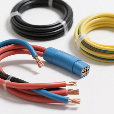
LISUN’s cable and wire test solutions meet IEC 60245-1, IEC 60227-1, IEC 60502-1 and IEC 60189 standards, covering electrical, mechanical, and safety tests for global compliance.

LISUN has all equipment according to the IEC60669 measurement, including environmental chamber, IP code waterproof dustproof test, switch lift test, etc.

Lisun can supply full test solutions for fluorescent lamp, including integrating sphere system, goniophotometer system, EMI EMC test, electronic ballast tester, electrical safety test, etc.

For the CFL design and manufactory, LISUN can supply a full quality control test solution, including photometric, colorimetric, electricity, flicker, IES candela distribution, surge test, electrical...

LISUN’s LED driver test solutions cover lab testing, online testing, EMC/EMI tests, and safety checks, meeting IEC 60335, UL 60335 standards for reliable performance evaluation.


 中文简体
中文简体