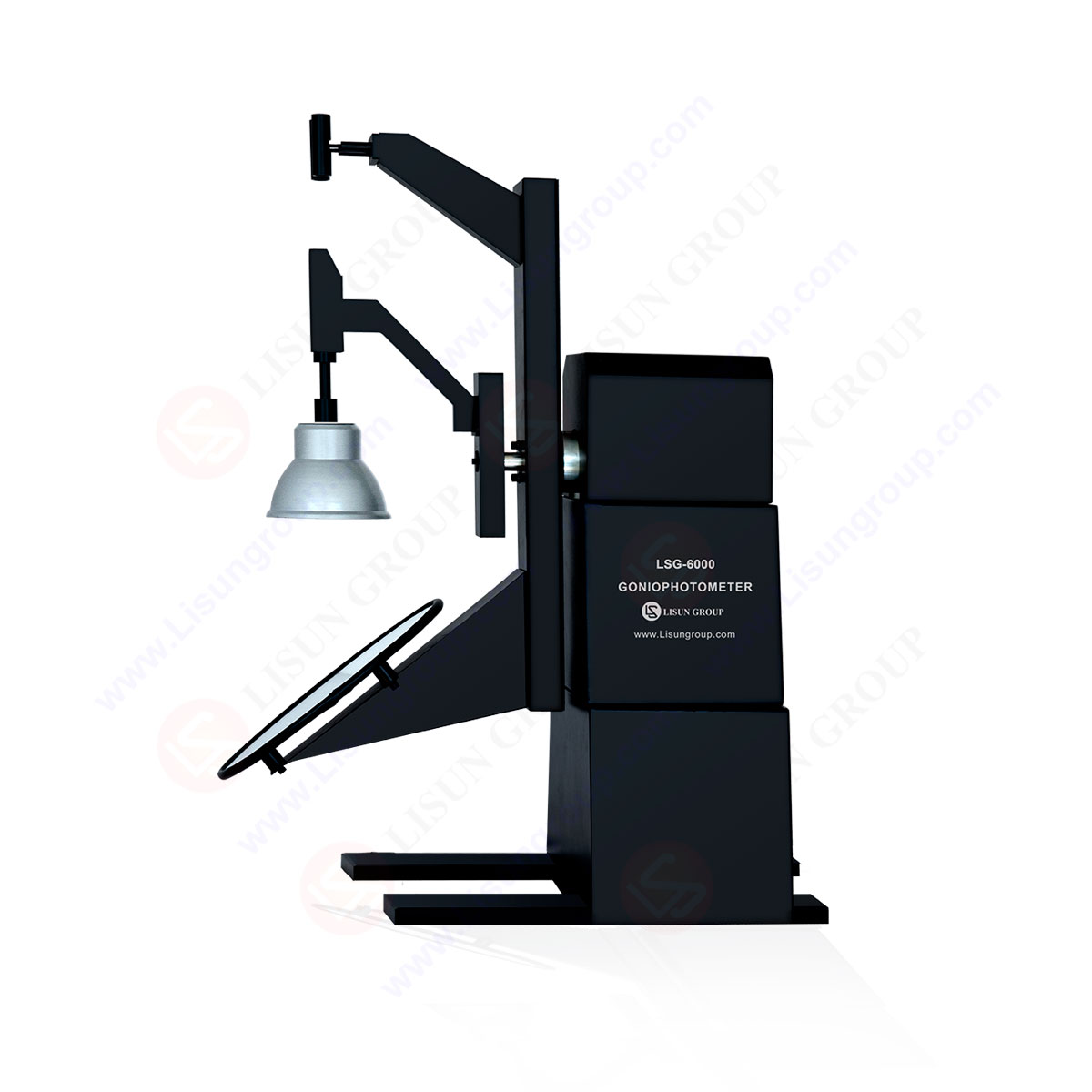
LM-79 Moving Detector Goniophotometer (Mirror Type C)
LSG-6000
High Precision Rotation Luminaire Goniophotometer
LSG-1890B
High Precision Rotation Luminaire Goniospectroradiometer
LSG-1890BCCD
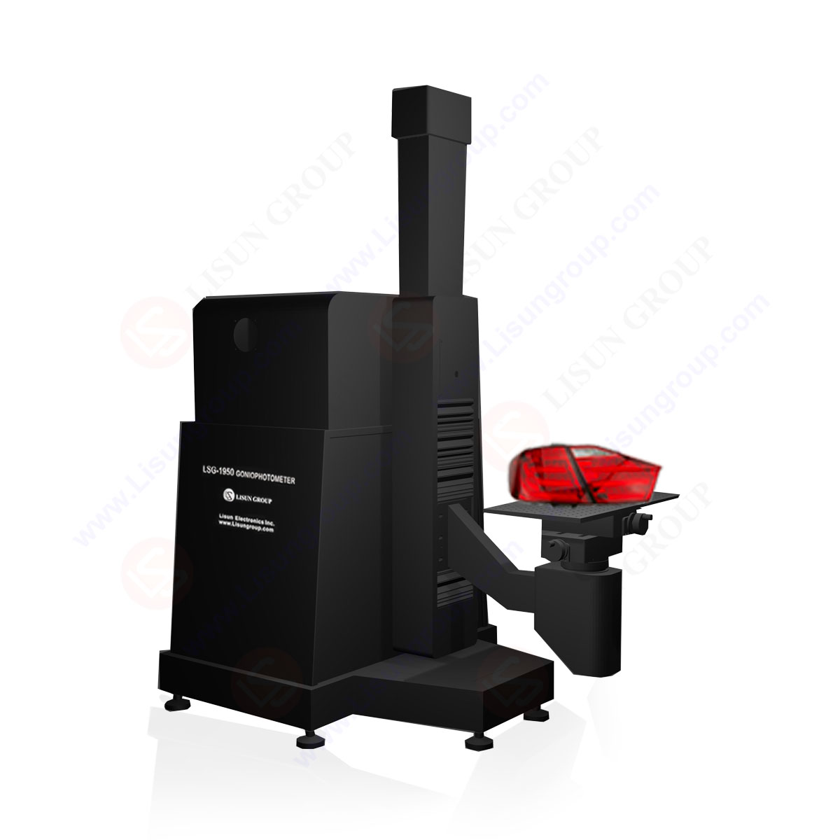
Goniophotometer for Automotive and Signal Lamps
LSG-1950
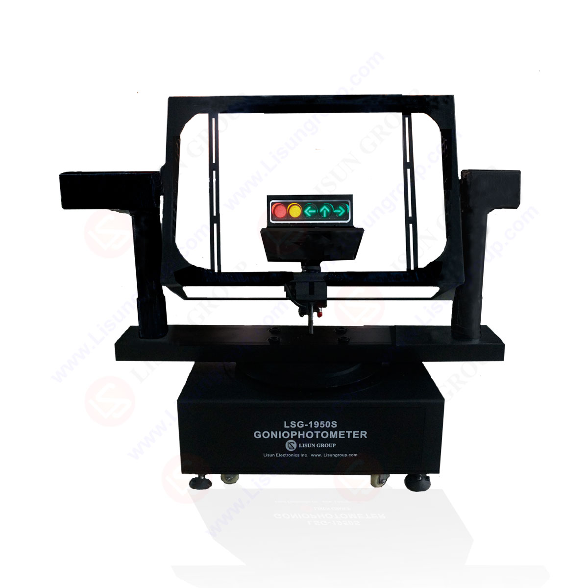
Goniophotometer for Traffic Signal Lamps
LSG-1950S
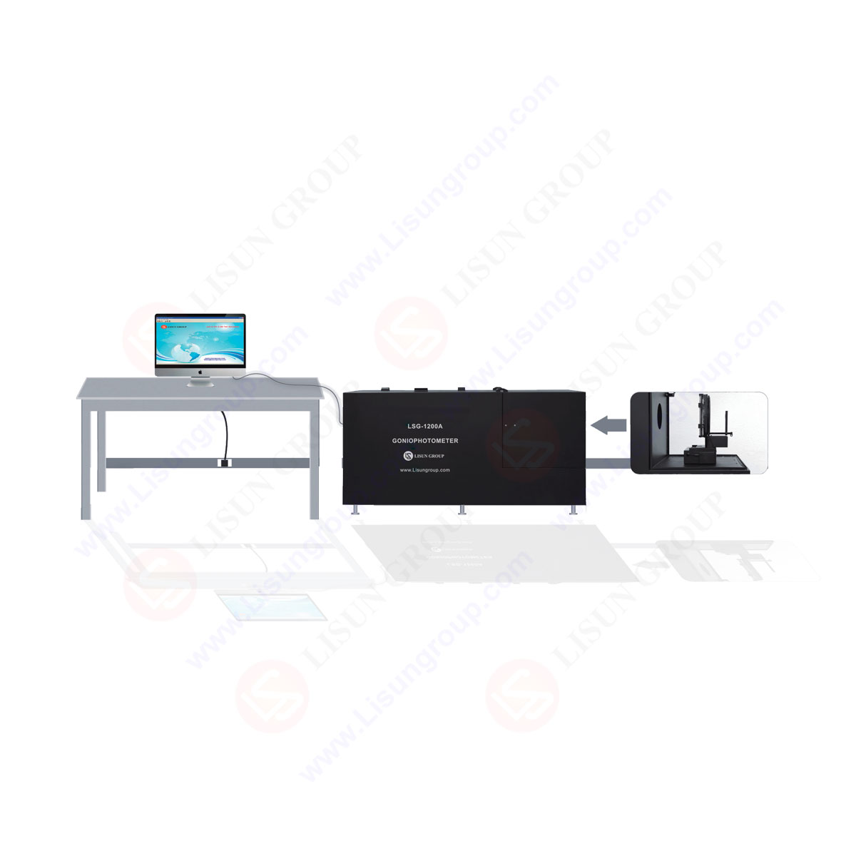
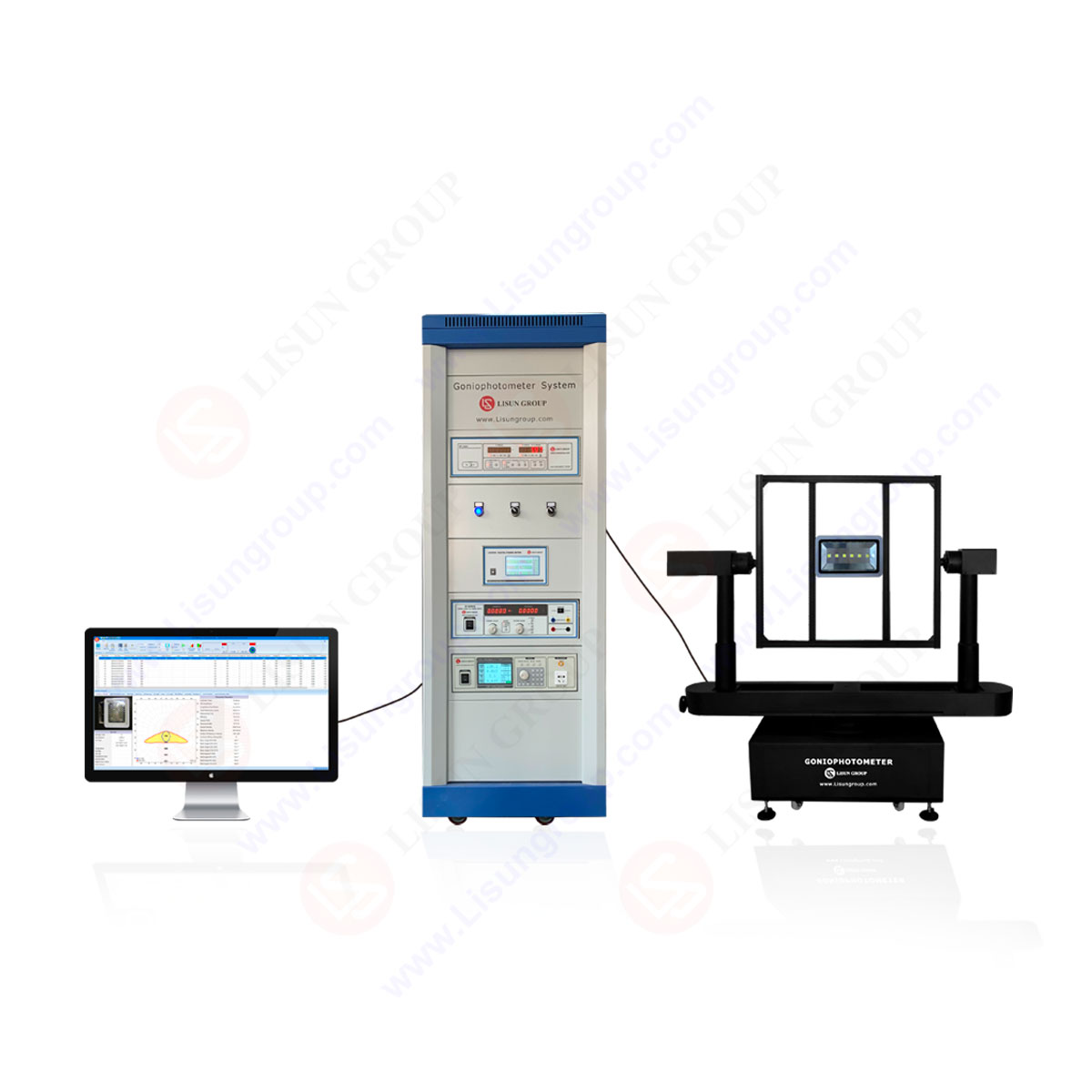
Compact Goniophotometer
LSG-1200A

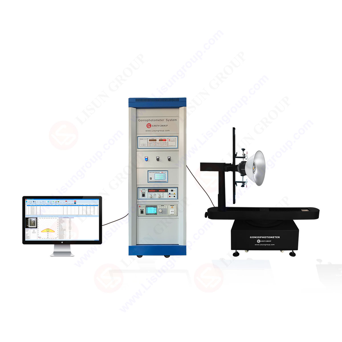
Near Field Moving Detector Goniophotometer
LSG-1900B
Select an organization
to browse standards
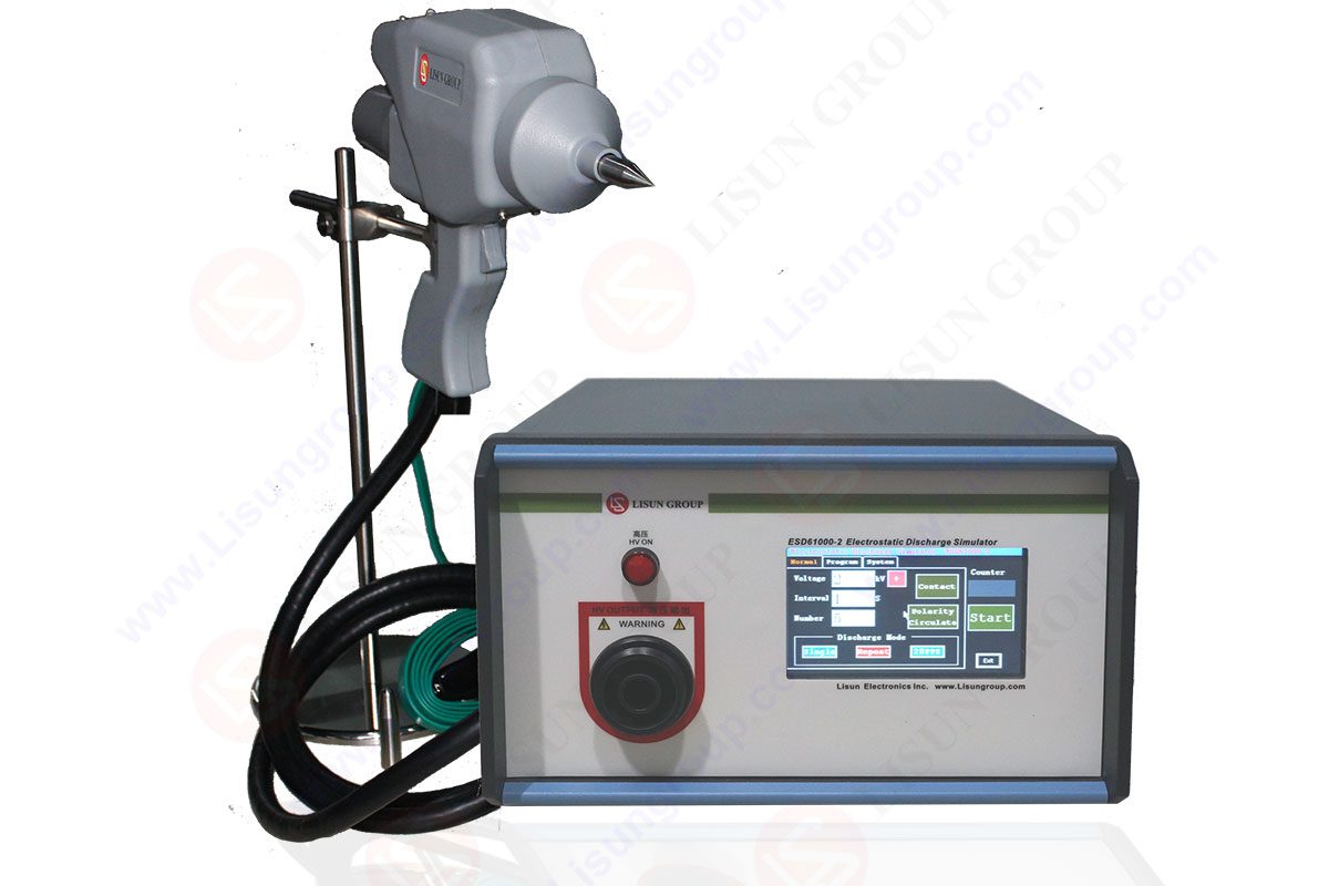
1. Countermeasures and rectification measures for common problems in ESD immunity testing
1.1 The mechanism of electrostatic discharge formation and its harm to electronic products
Static electricity is formed by the accumulation of positive and negative charges on two objects when two substances with different dielectric constants rub against each other. As far as the human body is concerned, the static electricity generated by the friction between the clothes and the skin is one of the main reasons for the electrification of the human body. When an electrostatic source is in contact with other objects, there is a flow of charge to counteract the voltage. The transmission of this high-speed power will generate potentially damaging voltages, currents and electromagnetic fields, which is electrostatic discharge.
 immunity Testing to IEC EN 61000-4-2 - LISUN")
In the production and use of electronic products, the operator is the most active source of static electricity, and may accumulate a certain amount of charge. When the human body touches the components and devices connected to the ground, electrostatic discharge will be generated. Electrostatic discharge is generally represented by ESD. Electrostatic discharge occurs when components and devices connected to ground are touched. Electrostatic discharge is generally represented by ESD. ESD can cause serious damage or malfunction of electronic equipment.
Most semiconductor devices are easily damaged by electrostatic discharge, especially LSI devices are more fragile. There are two kinds of damage caused by static electricity to the device, explicit and implicit. Hidden damage was not visible at the time, but the device became more fragile and easily damaged under conditions such as overvoltage and high temperature.
The two main damage mechanisms of ESD are thermal failure of the device due to heat generated by the ESD current and insulation breakdown due to the high voltage induced by ESD. In addition to easily causing circuit damage, ESD can also interfere with electronic circuits. There are two ways to interfere with ESD circuits.
One is the conduction method. If a certain part of the circuit forms a discharge path, that is, the ESD is connected to the circuit in the device, and the ESD current flows through the input end of the integrated chip, causing interference.
Another form of ESD interference is radiated interference. That is, a peak current is generated along with sparks during electrostatic discharge, and this current contains abundant high-frequency components. This produces a radiated magnetic field and an electric field, which can induce interfering electromotive forces in various signal loops of nearby circuits. The interference electromotive force is likely to exceed the threshold level of the logic circuit, causing false triggering. The magnitude of radiated interference also depends on the distance of the circuit from the point of electrostatic discharge. The magnetic field produced by ESD decays with the square of the distance. . The electric field produced by ESD decays cubed with distance. When the distance is close, both the electric field and the magnetic field are strong. When ESD occurs, circuits in nearby locations are generally affected.
ESD In the near field, the basic mode of radiative coupling can be capacitive or inductive, depending on the impedance of the ESD source and receiver. In the far field, there is electromagnetic field coupling.
The ESD-related electromagnetic interference (EMI) energy ceiling frequency can exceed 1GHz. At this frequency, typical equipment cables or even printed board traces can become very effective receive antennas. Thus, for typical analog or digital electronic equipment, ESD induces high levels of noise.
Generally speaking, to cause damage, ESD sparks must directly contact circuit wires, and radiative coupling usually only causes malfunction.
Under the effect of ESD, the devices in the circuit are more vulnerable to the energized condition than the unenergized condition.
2. Electrostatic discharge test and related requirements of electronic products
The requirements for the ESD immunity test are different for electronic product standards with different use environments, different uses and different ESD sensitivities, but most of these standards directly or indirectly refer to GB/T17626.2- 1998 (idt IEC 61000-4-2:1995): “Electrostatic Discharge Immunity Test of Electromagnetic Compatibility Test and Measurement Technology”, the national basic standard for electromagnetic compatibility, and the test is carried out according to the test method. The following briefly introduces the content, test methods and related requirements of the standard.
 immunity Testing to IEC EN 61000-4-2 1")
ESD61000-2_Electrostatic Discharge Simulator
2.1 Test objects:
This standard covers devices, systems, subsystems and external equipment in electrostatic discharge environments and installation conditions.
2.2 Test content:
There are various causes of electrostatic discharge, but this standard mainly describes the accumulation of static electricity by the operator through factors such as friction under low humidity conditions. Immunity requirements and test methods for electronic and electrical equipment subjected to electrostatic discharge directly from the operator and to adjacent objects.
2.3. Test purposes:
Test the ability of a single device or system to resist electrostatic interference. It simulates: (1) the discharge of the operator or object when touching the equipment. (2) Discharge of a person or object to an adjacent object.
2.4. Experiment method:
There are two test methods specified in this standard: contact discharge method and air discharge method. Contact discharge is the preferred test method, and air discharge is used where contact discharge cannot be used.
Contact discharge method: A test method in which the electrodes of the test generator are kept in contact with the equipment under test and the discharge is excited by the discharge switch in the generator.
Air discharge method: A test method in which the charging electrode of the test generator is brought close to the device under test and the device under test is excited to discharge by a spark.
2.5 Test environment:
This standard specifies the environmental conditions for air discharge:
Ambient temperature: 15℃~35℃, relative humidity: 30%~60%RH, atmospheric pressure: 86kPa~106kPa
The standard does not specify specific environmental conditions for contact discharges.
2.6. Test implementation:
Implementation site: The direct discharge is applied to the points or surfaces that the operator may touch during normal use of the equipment under test; the indirect discharge is applied to the horizontal coupling plate and the vertical coupling plate.
Direct discharge simulates the electrostatic discharge that occurs when an operator makes direct contact with the device under test. Indirect discharges discharge the horizontal and vertical coupling plates, simulating what happens when an operator discharges objects placed or installed near the device under test.
When direct discharge, contact discharge is the preferred form; only in places where contact discharge cannot be used (such as the surface is coated with an insulating layer, computer keyboard gaps, etc.), the air gap (air) discharge is used instead. Indirect discharge: choose the contact discharge method.
The test voltage shall be gradually increased to the specified value from low to high.
Different product or product family standards may have specific provisions for the implementation of tests according to the characteristics of the product.
2.7 Test results:
If the electrostatic discharge test fails, the following consequences may occur:
(1) Damage to semiconductor devices is directly caused by energy exchange.
(2) The electric field and magnetic field caused by the discharge change, resulting in the malfunction of the equipment.
 immunity Testing to IEC EN 61000-4-2 2")
ESD61000-2 Electrostatic Discharge Generator Discharge Current Waveform
3. Electrostatic discharge countermeasures and improvement points for electronic products:
There are many ways to reduce the impact of ESD-generated electromagnetic interference (EMI) on an electronic product or device: completely blocking ESD generation, preventing EMI (specifically EMI due to ESD in this article) from coupling into the circuit or device, and increasing the inherent EMI of the device through the design process. ESD immunity.
ESD usually occurs on conductive objects to which the product itself is exposed, or on adjacent conductive objects. For equipment, the parts that are prone to electrostatic discharge are: cables, keyboards, exposed metal frames, and holes, holes, and gaps on the equipment shell.
A common improvement method is to set up transient protection circuits between the product ESD occurrence or intrusion danger point, such as the input point and the ground, these circuits only function when the ESD induced voltage exceeds the limit. The protection circuit may include a plurality of current shunt units.
There are a variety of circuits that can achieve the purpose of ESD protection, but the following principles must be considered when selecting, and a trade-off between performance and cost: the speed is fast, which is determined by the characteristics of ESD interference; it can cope with the passage of large current; consider Transient voltage will occur in both positive and negative polarities; the capacitive and resistive effects of signal increase are controlled within the allowable range; volume factors are considered; product cost factors are considered.
4. General ESD Countermeasure Guidelines:
(1) Add protection diodes to susceptible CMOS and MOS devices;
(2) String tens of ohm resistors or ferrite beads on the susceptible transmission line (including the ground wire);
(3) Using electrostatic protection surface coating technology to make it difficult for ESD to discharge the core, which has been proved to be very effective;
(4) Try to use shielded cables;
(5) Install the filter at the susceptible interface; isolate the sensitive interface where the filter cannot be installed;
(6) Select a logic circuit with low pulse frequency;
(7) Shell shield and good grounding
Lisun Instruments Limited was found by LISUN GROUP in 2003. LISUN quality system has been strictly certified by ISO9001:2015. As a CIE Membership, LISUN products are designed based on CIE, IEC and other international or national standards. All products passed CE certificate and authenticated by the third party lab.
Our main products are Goniophotometer, Integrating Sphere, Spectroradiometer, Surge Generator, ESD Simulator Guns, EMI Receiver, EMC Test Equipment, Electrical Safety Tester, Environmental Chamber, Temperature Chamber, Climate Chamber, Thermal Chamber, Salt Spray Test, Dust Test Chamber, Waterproof Test, RoHS Test (EDXRF), Glow Wire Test and Needle Flame Test.
Please feel free to contact us if you need any support.
Tech Dep: Service@Lisungroup.com, Cell/WhatsApp:+8615317907381
Sales Dep: Sales@Lisungroup.com, Cell/WhatsApp:+8618117273997

LISUN’s Motor-Operated Tool | Power Tool Testing solutions strictly comply with a range of core international standards, providing full support for safety and electromagnetic compatibility (EMC)...
LISUN’s electric toy testing solutions cover IEC 62115, EN 71-1, ASTM F963 standards. Including electrical, mechanical, flammability tests to ensure toy safety compliance globally.
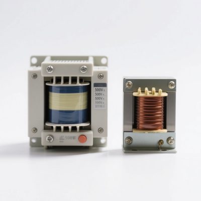
LISUN’s transformer test solutions meet IEC 61558-1, IEC 60076-1, IEC 62041 standards. Covering safety, performance, EMC tests, ensuring transformers comply with global requirements.

LISUN’s energy meter testing solutions align with IEC 62052-11, IEC 62053 series standards. Covering safety, electrical, environmental, and EMC tests, we help manufacturers meet global compliance...
LISUN’s household and appliance switch testing solutions meet IEC 60669, IEC 61058, IEC 62271 standards. Covering electrical, mechanical & EMC tests for global compliance.

LISUN’s automotive electronics test solutions cover photometric/colorimetric testing, EMC immunity tests, IP waterproof/dustproof tests, and environmental simulation, meeting ISO, SAE, ECE standards.
LISUN has all equipment according to the IEC60669 measurement, including environmental chamber, IP code waterproof dustproof test, switch lift test, etc.

Lisun can supply full test solutions for fluorescent lamp, including integrating sphere system, goniophotometer system, EMI EMC test, electronic ballast tester, electrical safety test, etc.

For the CFL design and manufactory, LISUN can supply a full quality control test solution, including photometric, colorimetric, electricity, flicker, IES candela distribution, surge test, electrical...

LISUN’s LED driver test solutions cover lab testing, online testing, EMC/EMI tests, and safety checks, meeting IEC 60335, UL 60335 standards for reliable performance evaluation.

 中文简体
中文简体