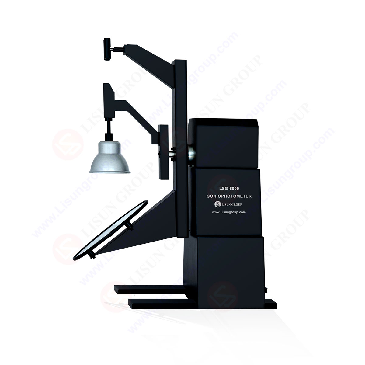
LM-79 Moving Detector Goniophotometer (Mirror Type C)
LSG-6000
High Precision Rotation Luminaire Goniophotometer
LSG-1890B
High Precision Rotation Luminaire Goniospectroradiometer
LSG-1890BCCD
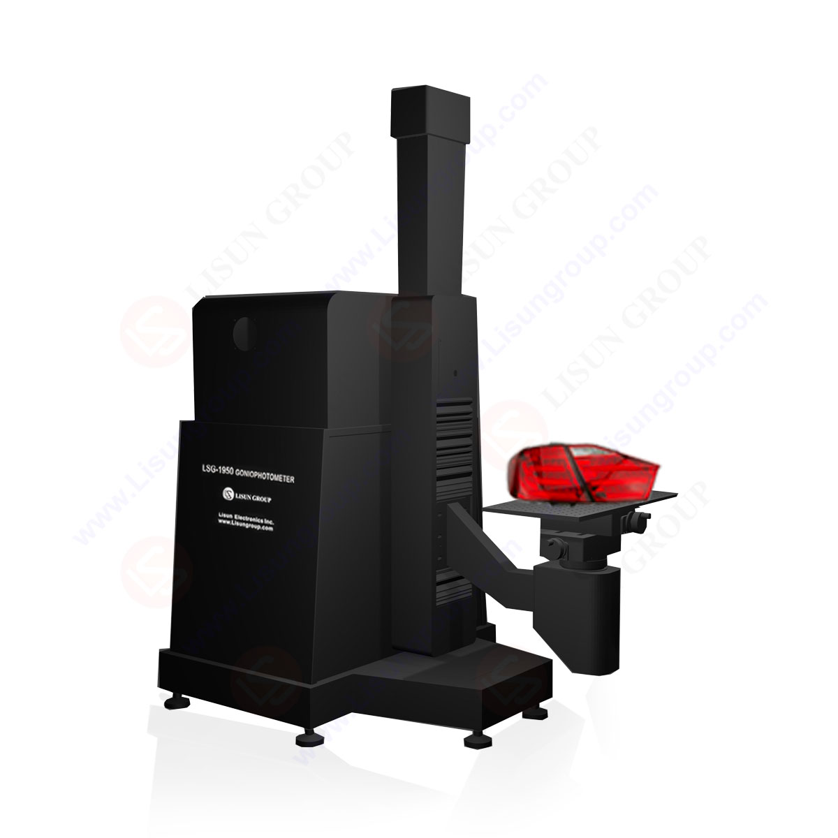
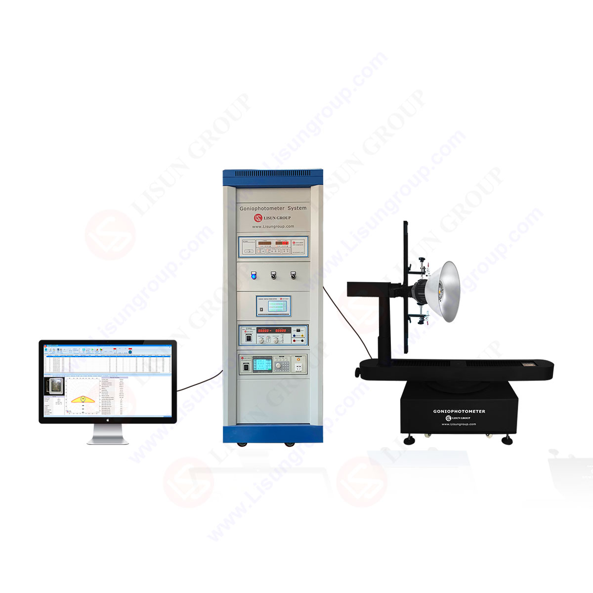
Goniophotometer for Automotive and Signal Lamps
LSG-1950
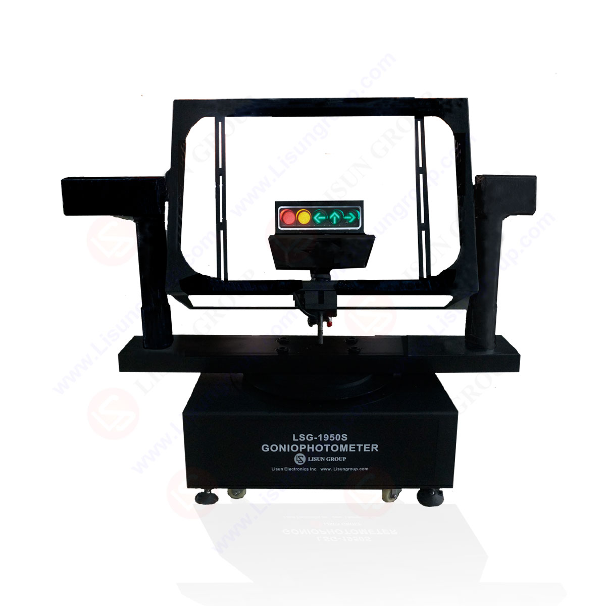
Goniophotometer for Traffic Signal Lamps
LSG-1950S
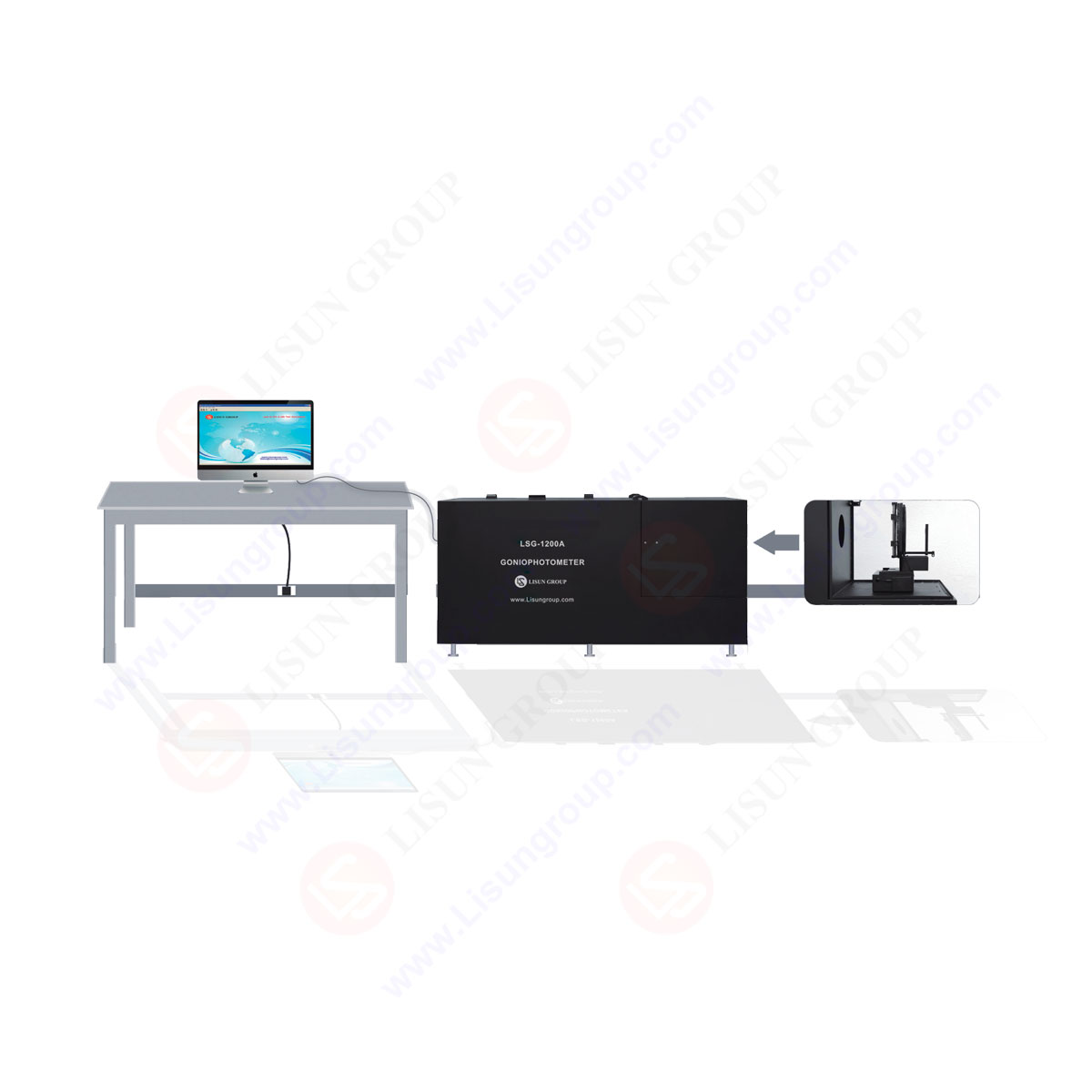
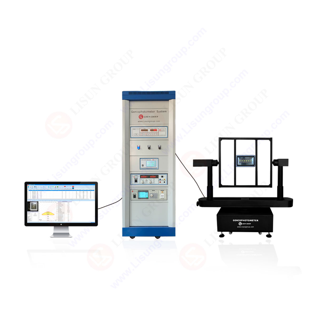
Compact Goniophotometer
LSG-1200A

Near Field Moving Detector Goniophotometer
LSG-1900B
Select an organization
to browse standards
A key design challenge in designing a power bank is passing EMI testing. Electronics engineers often worry about failing EMI tests. If the circuit EMI test fails many times, it will be a nightmare. You will have to work around the clock in the EMI lab to fix problems and avoid delays in product rollouts. For consumer products such as power banks, the design cycle is short and the EMI certification restrictions are strict, so you want to add enough EMI filters to pass the EMI test smoothly, but you don’t want to increase the space and add too much cost to the circuit . It seems difficult to juggle both.

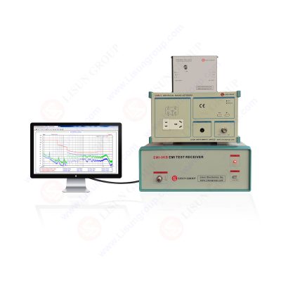
EMI-9KB_EMI Receiver System
The TI design Low Radiated EMI Boost Converter Reference Design (PMP9778) provides such a solution. It can support 2.7 – 4.4V input voltage, 5V / 3A, 9V / 2A and 12V / 1.5A output power, and is only suitable for power bank applications. With placement and layout optimization, this TI design achieves 6 dB more headroom than in EN55022 and CISPR22 Class B radiated tests. Let’s take a look at the design process.
Identify critical current paths
EMI starts with a high instantaneous rate of current change (di/dt) cycling. Therefore, we should distinguish high di/dt critical paths at the beginning of the design. To achieve these goals, it is important to understand the current conduction paths and signal flow in switching power supplies.
Figure 1 shows the boost converter topology and critical current paths. When S2 is closed and S1 is open, AC current flows through the blue loop. When S1 is closed and S2 is open, AC current flows through the green loop. Therefore, the current flows through the input capacitor Cin, and the inductor L is a continuous current, while the current flows through S2, S1, and the output capacitor Cout is a pulsating current (red loop). Therefore, we define the red loop as the critical current path. This path has the highest EMI energy. During placement, we should minimize the area enclosed by it.

Figure 1 Critical current path for a boost converter
Minimize loop area for high di/dt paths
Figure 2 shows the pin configuration of the TPS61088. Figure 3 shows an example layout of the critical current paths for the TPS61088. The NC pin indicates that there is no connection inside the device. Therefore, they can be connected to PGND. Electrically, connecting the two NC pins to the PGND ground plane facilitates heat dissipation and reduces the impedance of the return path. From an EMI perspective, connecting the two NC pins to the PGND ground plane brings the VOUT and PGND planes of the TPS61088 closer to each other. This makes the placement of the output capacitors easier. As can be seen from Figure 3, placing a 0603 1-UF (or 0402 1-UF) high frequency ceramic capacitor COUT_HF as close as possible to the VOUT pin results in the smallest area of the high di/dt loop.

Figure 2 TPS61088 pin configuration

Figure 3 TPS61088 critical path layout example
The maximum electric field strength from a high di/di loop at a distance of 10 meters from the ground plane can be calculated by the following formula:

Figure 4 shows the radiated EMI results with and without COUT_HF. Under the same test conditions, the radiated EMI is improved by 4dBuV/m with COUT_HF.

Figure 4. Radiated EMI Results with and Without COUT_HF
Place a ground plane under the critical path
High tracking inductance results in poor radiated EMI. Because the magnetic field strength is proportional to the inductance. Placing a fixed ground plane on the next layer of the critical trace can solve this problem.
Table 1 gives the given tracking inductances on different PCB boards. We can see that for a four-layer PCB with a 0.4 mm insulation thickness between the signal layer and the ground plane, the tracking inductance is much smaller than the tracking inductance for a 1.2 mm thick 2-layer PCB. Therefore, placing the shortest fixed ground plane in the critical path is one of the most effective ways to reduce EMI.
Figure 5 shows the radiated EMI results for a 2-layer PCB and a 4-layer PCB. Based on the same layout and the same test conditions, radiated EMI can be improved by 10dBuV/m over a 4-layer PCB.

Figure 5 Radiated EMI results for a 2-layer PCB and a 4-layer PCB
Add RC buffer
If the radiated levels still exceed the required levels and the layout cannot be improved any further, adding an RC snubber and power ground to the TPS61088 SW pin can help reduce radiated EMI levels. The RC snubber should be placed as close as possible to the switch node and power ground. It can effectively suppress the SW voltage loop, which means that the radiated EMI is improved at the ringing frequency.
Lisun Instruments Limited was found by LISUN GROUP in 2003. LISUN quality system has been strictly certified by ISO9001:2015. As a CIE Membership, LISUN products are designed based on CIE, IEC and other international or national standards. All products passed CE certificate and authenticated by the third party lab.
Our main products are Goniophotometer, Integrating Sphere, Spectroradiometer, Surge Generator, ESD Simulator, EMI Receiver, EMC Test Equipment, Electrical Safety Tester, Environmental Chamber, Temperature Chamber, Climate Chamber, Thermal Chamber, Salt Spray Test, Dust Test Chamber, Waterproof Test, RoHS Test (EDXRF), Glow Wire Test and Needle Flame Test.
Please feel free to contact us if you need any support.
Tech Dep: Service@Lisungroup.com, Cell/WhatsApp:+8615317907381
Sales Dep: Sales@Lisungroup.com, Cell/WhatsApp:+8618917996096

LISUN’s Motor-Operated Tool | Power Tool Testing solutions strictly comply with a range of core international standards, providing full support for safety and electromagnetic compatibility (EMC)...
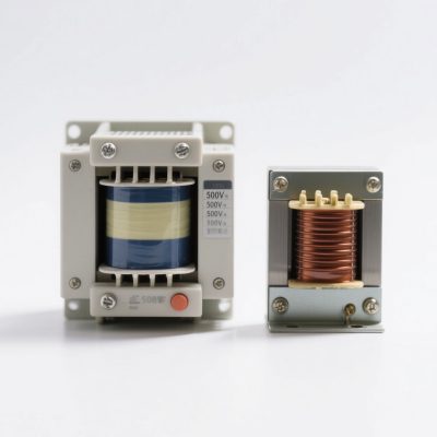
LISUN’s transformer test solutions meet IEC 61558-1, IEC 60076-1, IEC 62041 standards. Covering safety, performance, EMC tests, ensuring transformers comply with global requirements.
LISUN’s household and appliance switch testing solutions meet IEC 60669, IEC 61058, IEC 62271 standards. Covering electrical, mechanical & EMC tests for global compliance.

For the CFL design and manufactory, LISUN can supply a full quality control test solution, including photometric, colorimetric, electricity, flicker, IES candela distribution, surge test, electrical...


 中文简体
中文简体