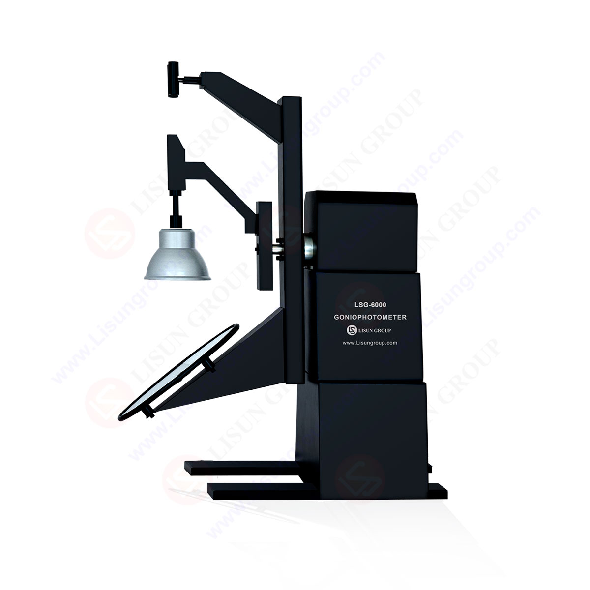
LM-79 Moving Detector Goniophotometer (Mirror Type C)
LSG-6000
High Precision Rotation Luminaire Goniophotometer
LSG-1890B
High Precision Rotation Luminaire Goniospectroradiometer
LSG-1890BCCD
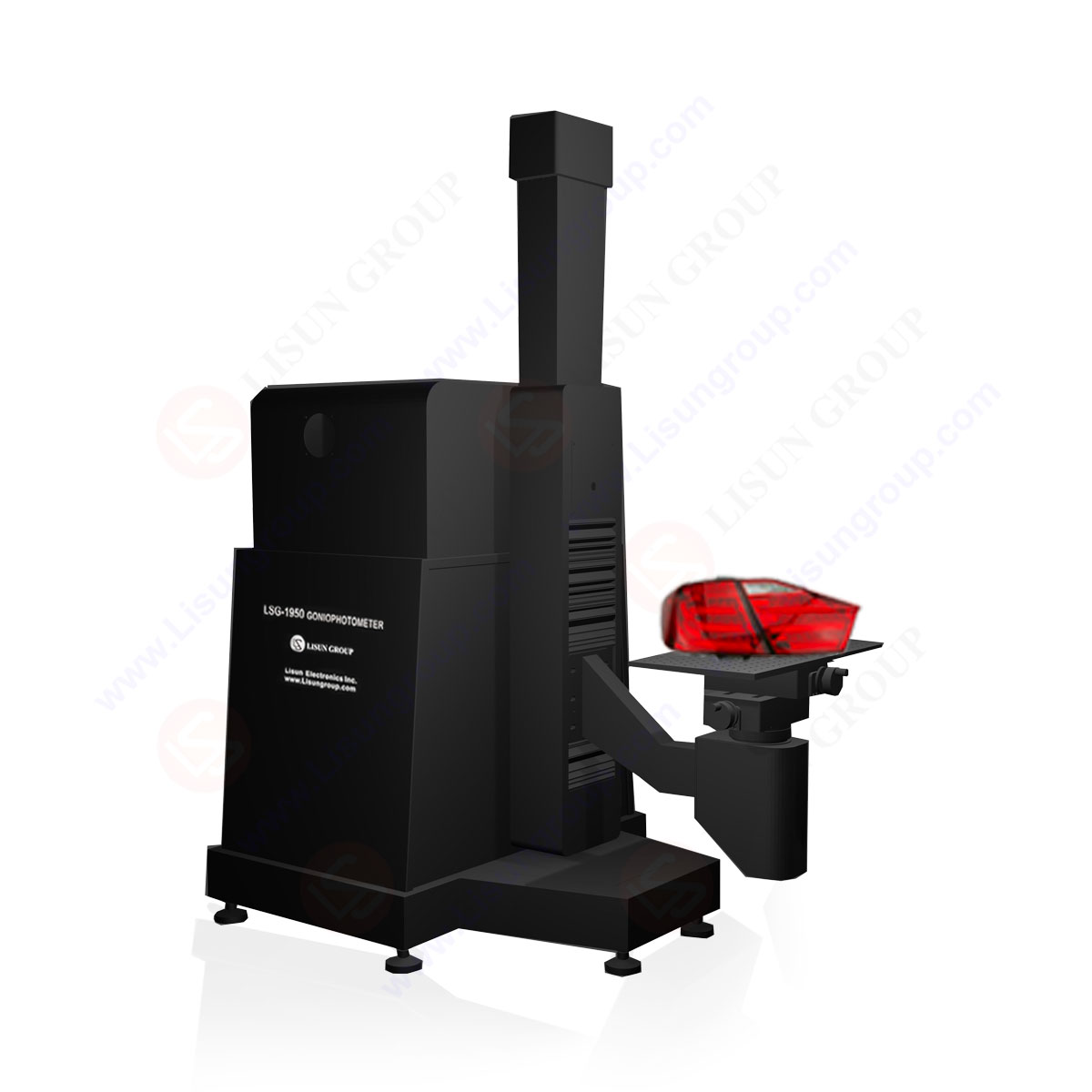
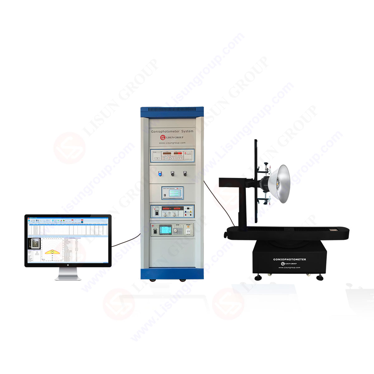
Goniophotometer for Automotive and Signal Lamps
LSG-1950
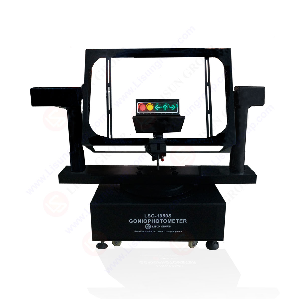
Goniophotometer for Traffic Signal Lamps
LSG-1950S
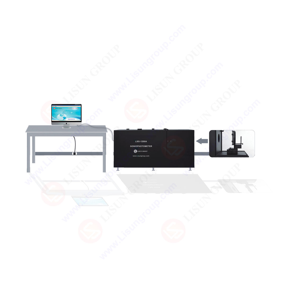
Compact Goniophotometer
LSG-1200A

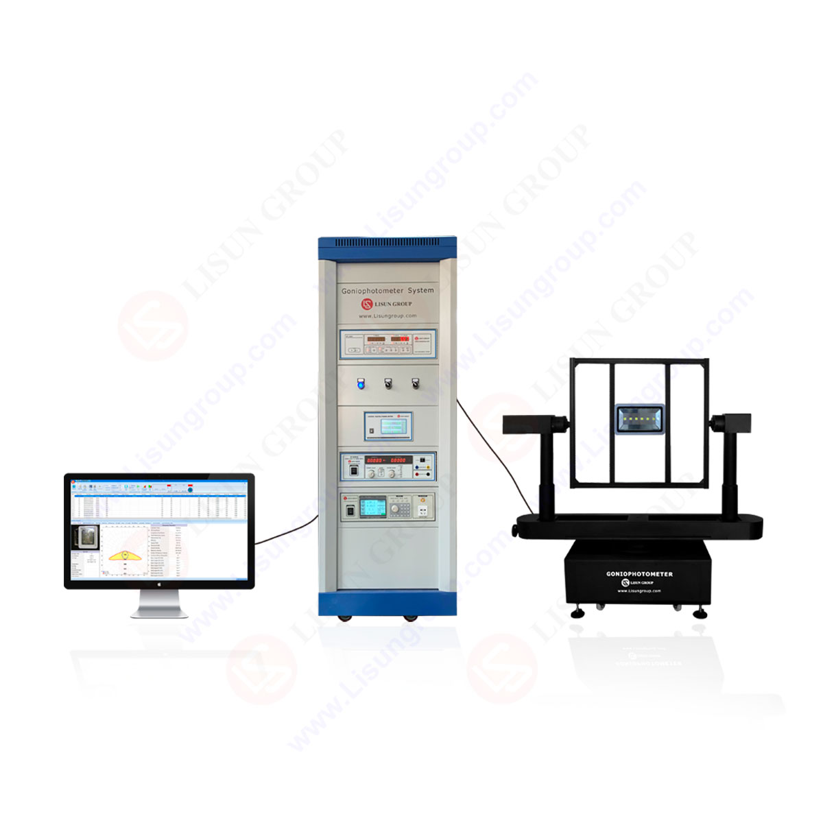
Near Field Moving Detector Goniophotometer
LSG-1900B
Select an organization
to browse standards
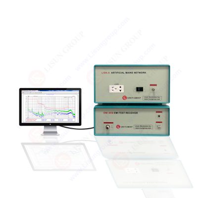
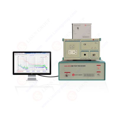
At present, the problem of electromagnetic compatibility of electronic products has attracted more and more attention. Especially developed countries in the world have formed a complete electromagnetic compatibility system. At the same time, our country is also establishing an electromagnetic compatibility system. Therefore, the realization of EMI testing of products is a passport to enter the international market. LISUN EMI Test System EMI-9KB fully meets CISPR15:2018, CISPR16-1, GB17743, FCC, EN55015 and EN55022.

For the switching power supply, since the switching tube and rectifier tube work under the condition of high current and high voltage, it will produce strong electromagnetic interference to the outside world, so the conduction emission and electromagnetic radiation emission of the switching power supply are more difficult than other products. To achieve electromagnetic compatibility, but if we have a clear understanding of the principle of electromagnetic interference generated by switching power supplies, it is not difficult to find suitable countermeasures to reduce the conducted emission level and radiated emission level to an appropriate level to achieve electromagnetic compatibility design.

EMI Testing Application
The Generation Mechanism and Propagation way of Electromagnetic Interference in Switching Power Supply
The high switching action of power switching devices is the main cause of electromagnetic interference (EMI) in switching power supplies. The increase of switching frequency reduces the size and weight of the power supply on the one hand, and leads to more serious EMI problems on the other hand. Electromagnetic interference in switching power supplies is divided into two types: conducted interference and radiated interference. Usually conducted interference is better analyzed, and circuit theory and mathematical knowledge can be combined to study the characteristics of various components in electromagnetic interference; but for radiated interference, due to the comprehensive effect of different interference sources in the circuit, it also involves to the electromagnetic field theory, it is more difficult to analyze. The mechanism of these two interferences will be briefly introduced below. Conducted interference can be divided into common mode (Common Mode-CM) interference and differential mode (Differential Mode-DM) interference. Due to the existence of parasitic parameters and the high-frequency turn-on and turn-off of switching devices in the switching power supply, the switching power supply generates large common-mode interference and differential-mode interference at its input (ie, the AC grid side).
Common Mode (CM) Interference
When the converter works at high frequency, due to the high dv/dt, the parasitic capacitance between the transformer coils and between the switch tube and the heat sink is excited, resulting in common mode interference.
According to the principle of common mode interference, the following suppression methods are often used in practical applications:
1. Optimize the layout of circuit components to minimize parasitic and coupling capacitances.
2. Delay the turn-on and turn-off time of the switch. But this is inconsistent with the trend of high frequency switching power supply.
3. Apply a snubber circuit to slow down the rate of change of dv/dt.
Differential Mode (DM) Interference
The current in the switching converter is switched at high frequency, resulting in a high di/dt on the input and output filter capacitors, that is, the interference voltage is induced on the equivalent inductance or impedance of the filter capacitor. At this time, differential mode interference will occur. Therefore, the selection of high-quality filter capacitors (equivalent inductance or impedance is very low) can reduce differential mode interference.
Generation and propagation of radiated interference
Radiation interference can be further divided into near-field interference (distance between measurement point and field source <λ/6 (λ is the wavelength of the interference electromagnetic wave)) and far-field interference (distance between measurement point and field source>λ/6). According to Maxwell’s electromagnetic field theory, a changing current in a conductor produces a changing magnetic field in the space around it, which in turn produces a changing electric field, both of which obey Maxwell’s equations. The magnitude and frequency of this changing current determine the magnitude and range of the electromagnetic field generated. In the radiation research, the antenna is the source of electromagnetic radiation. In the switching power supply circuit, the components and connections in the main circuit can be considered as the antenna, which can be analyzed by applying the theory of electric dipole and magnetic dipole. In the analysis, diodes, switching tubes, capacitors, etc. can be regarded as electric dipoles; inductive coils can be regarded as magnetic dipoles, and then comprehensive analysis can be carried out with the relevant electromagnetic field theory.
When the switching power supply is working, its internal voltage and current waveforms rise and fall in a very short time. Therefore, the switching power supply itself is a source of noise. The interference generated by the switching power supply can be divided into two types: peak interference and harmonic interference according to the type of noise interference source; if divided according to the coupling path, it can be divided into two types: conduction interference and radiation interference. The fundamental way to prevent the interference generated by the power supply from causing harm to the electronic system and the power grid is to weaken the noise source, or to cut off the coupling path between the power supply noise and the electronic system and the power grid.

Switching power supply
Explain separately according to the source of noise interference
1.Interference caused by the reverse recovery time of the diode
The AC input voltage is converted into a sinusoidal pulsating voltage by the power diode rectifier bridge, and then becomes DC after being smoothed by the capacitor, but the waveform of the capacitor current is not a sine wave but a pulse wave. It can be seen from the current waveform that the current contains higher harmonics. A large amount of current harmonic components flow into the power grid, causing harmonic pollution to the power grid. In addition, since the current is a pulse wave, the input power factor of the power supply is reduced. When the rectifier diode in the high-frequency rectifier circuit is forward-conducting, a large forward current flows. When it is turned off by the reverse bias voltage, due to the accumulation of more carriers in the PN junction, the current-carrying For a period of time before the carrier disappears, the current will flow in the opposite direction, resulting in a sharp decrease in the reverse recovery current of the carrier disappearance and a large current change (di/dt).

capacitor
2. Harmonic interference generated when the switch tube works
When the power switch tube is turned on, a large pulse current flows. For example, the input current waveform of forward type, push-pull type and bridge type converter is approximately rectangular wave when resistive load, which contains abundant high-order harmonic components. When zero-current, zero-voltage switching is used, this harmonic interference will be minimal. In addition, the sudden change of current caused by the leakage inductance of the high-frequency transformer winding during the off period of the power switch tube will also produce peak interference.

Harmonic interference generated when the switch tube
3. Interference caused by the AC input circuit
The rectifier tube at the input end of the switching power supply without a power frequency transformer will cause high-frequency damped oscillation during the reverse recovery period and cause interference. The peak interference and harmonic interference energy generated by the switching power supply, the interference formed through the input and output lines of the switching power supply is called conduction interference; and the energy of harmonic and parasitic oscillation, when propagated through the input and output lines, will be in the space. Generate electric and magnetic fields. This interference generated by electromagnetic radiation is called radiated interference.
4. Other reasons
The parasitic parameters of the components and the schematic design of the switching power supply are not perfect. The printed circuit board (PCB) wiring is usually arranged manually, which has great randomness. The near-field interference of the PCB is large, and the installation and unreasonable placement and orientation will cause EMI interference. This increases the difficulty of extracting PCB distribution parameters and estimating near-field interference.
The reaction of Flyback architecture noise on the spectrum
• The oscillation generated at 0.15MHz is the interference caused by the 3rd harmonic of the switching frequency;
• The oscillation generated at 0.2MHz is the interference caused by the superposition of the 4th harmonic of the switching frequency and the fundamental wave of Mosfet oscillation 2 (190.5KHz); so this part is stronger;
• The oscillation generated at 0.25MHz is the interference caused by the 5th harmonic of the •switching frequency;
• The oscillation generated at 0.35MHz is the interference caused by the 7th harmonic of the switching frequency;
• The oscillation generated at 0.39MHz is the interference caused by the superposition of the 8th harmonic of the switching frequency and the fundamental wave of Mosfet oscillation 2 (190.5KHz);
• The oscillation generated at 1.31MHz is the interference caused by the fundamental wave of Diode oscillation 1 (1.31MHz);
• The oscillation generated at 3.3MHz is the interference caused by the fundamental wave of Mosfet oscillation 1 (3.3MHz);
Characteristics of switching power supply EMI
As an energy conversion device working in the switching state, the voltage and current change rates of the switching power supply are very high, and the interference intensity is relatively large; the interference sources are mainly concentrated during the power switching period and the radiator and high-level transformer connected to it. The location of the circuit interference source is relatively clear; the switching frequency is not high (from tens of kilohertz and several megahertz), and the main forms of interference are conducted interference and near-field interference; and printed circuit board (PCB) traces are usually wired manually. Has greater randomness, which increases the difficulty of extracting PCB distribution parameters and near-field interference.
Measures to Prevent EMI When Designing Switching Power Supplies
• Minimize the area of PCB copper foil for noise circuit nodes, such as the drain, collector, primary and secondary winding nodes of switch tubes, etc.;
• Keep the input and output terminals away from noise components, such as transformer wire wraps, transformer cores, heat sinks of switch tubes, etc.;
• Keep noisy components (such as unshielded transformer wire wraps, unshielded transformer cores and switches, etc.) away from the edge of the enclosure, which is likely to be close to the outside ground wire under normal operation;
• If the transformer is not shielded with electric field, keep the shield and heat sink away from the transformer;
• Minimize the area of the following current loops: secondary (output) rectifiers, primary switching power devices, gate (base) drive lines, auxiliary rectifiers;
• Do not mix the gate (base) drive feedback loop with the primary switch circuit or auxiliary rectifier circuit;
• Adjust and optimize the damping resistance value so that it does not produce ringing sound during the dead time of the switch;
• Prevent EMI filter inductor saturation;
• Keep the turning nodes and components of the secondary circuit away from the shield of the primary circuit or the heat sink of the switch;
• Keep primary circuit swing nodes and component bodies away from shields or heat sinks;
• Place the EMI filter for high frequency input close to the input cable or connector end;
• Keep the EMI filter of the high frequency output close to the output wire terminals;
• Keep a certain distance between the copper foil of the PCB on the opposite side of the EMI filter and the component body; put some resistors on the line of the rectifier of the auxiliary coil; connect damping resistors in parallel with the magnetic bar coil; connect both ends of the output RF filter in parallel Damping resistance;
• It is allowed to put a 1nF/500V ceramic capacitor or a series of resistors in the PCB design, which is connected across the primary static end of the transformer and the auxiliary winding;
• Keep the EMI filter away from the power transformer, especially at the end of the wrap;
• If the PCB area is sufficient, the pins for shielding windings and the position for placing RC dampers can be left on the PCB, and the RC dampers can be connected across both ends of the shielding windings;
• Place a small radial lead capacitor (Miller, 10 picofarads/1kV) between the drain and gate of the switching power FET if space permits;
• Put a small RC damper on the DC output if space permits;
• Do not place the AC socket against the heat sink of the primary switch.

EMI-9KB EMI Test Receiver
EMI countermeasures in radiation
Excessive broadband noise in the 30-300MHz frequency band
1. Verify by adding a decoupling magnetic ring (can be opened and closed) on the power line. If there is improvement, it means that it is related to the power line. The following rectification methods are used: If the device has an integrated filter, check whether the grounding of the filter is correct. Good, whether the ground wire is as short as possible;
2. The grounding of the filter with metal casing is preferably directly through the large area of bonding between the casing and the ground. Check whether the input and output lines of the filter are close to each other. Appropriately adjust the capacitance of the X/Y capacitor, the differential mode inductance and the inductance of the common mode choke coil; pay attention to safety issues when adjusting the Y capacitor; changing the parameters may improve the radiation of a certain section, but it will lead to other frequency changes. Poor, so you need to keep trying to find the best combination. It is a good way to appropriately increase the resistance value on the trigger electrode; it can also be effectively reduced by connecting a small capacitor to the collector of the switching transistor (or the drain of the MOS transistor) or the secondary output rectifier to ground Common Mode Switching Noise.
3. The switching power supply board must control the return area of each loop during PCB wiring, which can greatly reduce the differential mode radiation. Add 104/103 capacitors to the PCB power traces for power decoupling; when wiring the multi-layer board, the power plane and the ground plane are required to be close to each other; set a magnetic ring on the power line for comparison and verification, which can be added on the single board later. Common mode inductors are used to achieve this, or a magnetic ring is injected on the cable. The length of the L line of the input AC line should be as short as possible; inside the shielding equipment, whether there is an interference source near the holes; whether there is insulating paint sprayed on the lap joints of the structural parts, use emery cloth to wipe off the insulating paint for a comparative test. Check whether the grounding screw is sprayed with insulating paint and whether the grounding is good.
Lisun Instruments Limited was found by LISUN GROUP in 2003. LISUN quality system has been strictly certified by ISO9001:2015. As a CIE Membership, LISUN products are designed based on CIE, IEC and other international or national standards. All products passed CE certificate and authenticated by the third party lab.
Our main products are Goniophotometer, Integrating Sphere, Spectroradiometer, Surge Generator, ESD Simulator Guns, EMI Receiver, EMC Test Equipment, Electrical Safety Tester, Environmental Chamber, Temperature Chamber, Climate Chamber, Thermal Chamber, Salt Spray Test, Dust Test Chamber, Waterproof Test, RoHS Test (EDXRF), Glow Wire Test and Needle Flame Test.
Please feel free to contact us if you need any support.
Tech Dep: Service@Lisungroup.com, Cell/WhatsApp:+8615317907381
Sales Dep: Sales@Lisungroup.com, Cell/WhatsApp:+8618117273997

LISUN’s Motor-Operated Tool | Power Tool Testing solutions strictly comply with a range of core international standards, providing full support for safety and electromagnetic compatibility (EMC)...
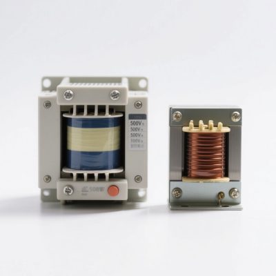
LISUN’s transformer test solutions meet IEC 61558-1, IEC 60076-1, IEC 62041 standards. Covering safety, performance, EMC tests, ensuring transformers comply with global requirements.
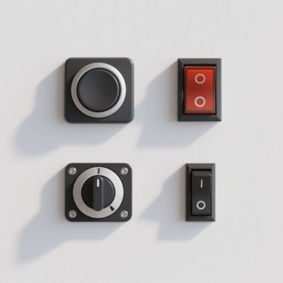
LISUN’s household and appliance switch testing solutions meet IEC 60669, IEC 61058, IEC 62271 standards. Covering electrical, mechanical & EMC tests for global compliance.

LISUN provide full test solutions for HID lamp, including integrating sphere system, goniophotometer system, EMI EMC chamber, HID ballast tester, electrical safety test, etc.

Lisun can supply full test solutions for fluorescent lamp, including integrating sphere system, goniophotometer system, EMI EMC test, electronic ballast tester, electrical safety test, etc.

For the CFL design and manufactory, LISUN can supply a full quality control test solution, including photometric, colorimetric, electricity, flicker, IES candela distribution, surge test, electrical...


 中文简体
中文简体