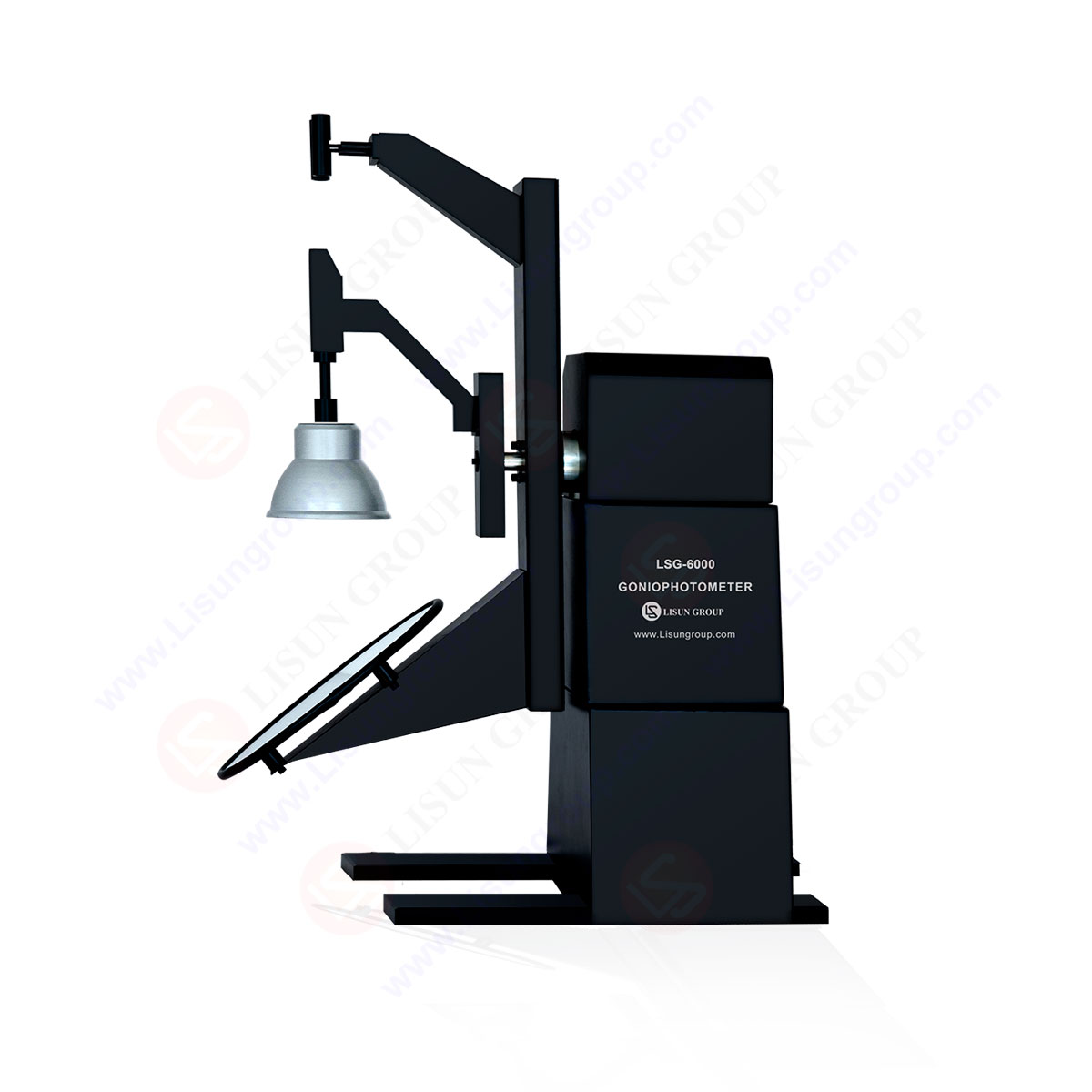
LM-79 Moving Detector Goniophotometer (Mirror Type C)
LSG-6000
High Precision Rotation Luminaire Goniophotometer
LSG-1890B
High Precision Rotation Luminaire Goniospectroradiometer
LSG-1890BCCD
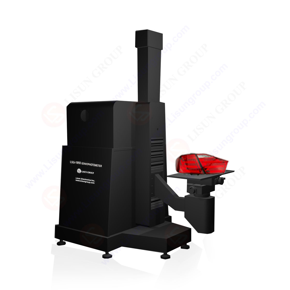
Goniophotometer for Automotive and Signal Lamps
LSG-1950
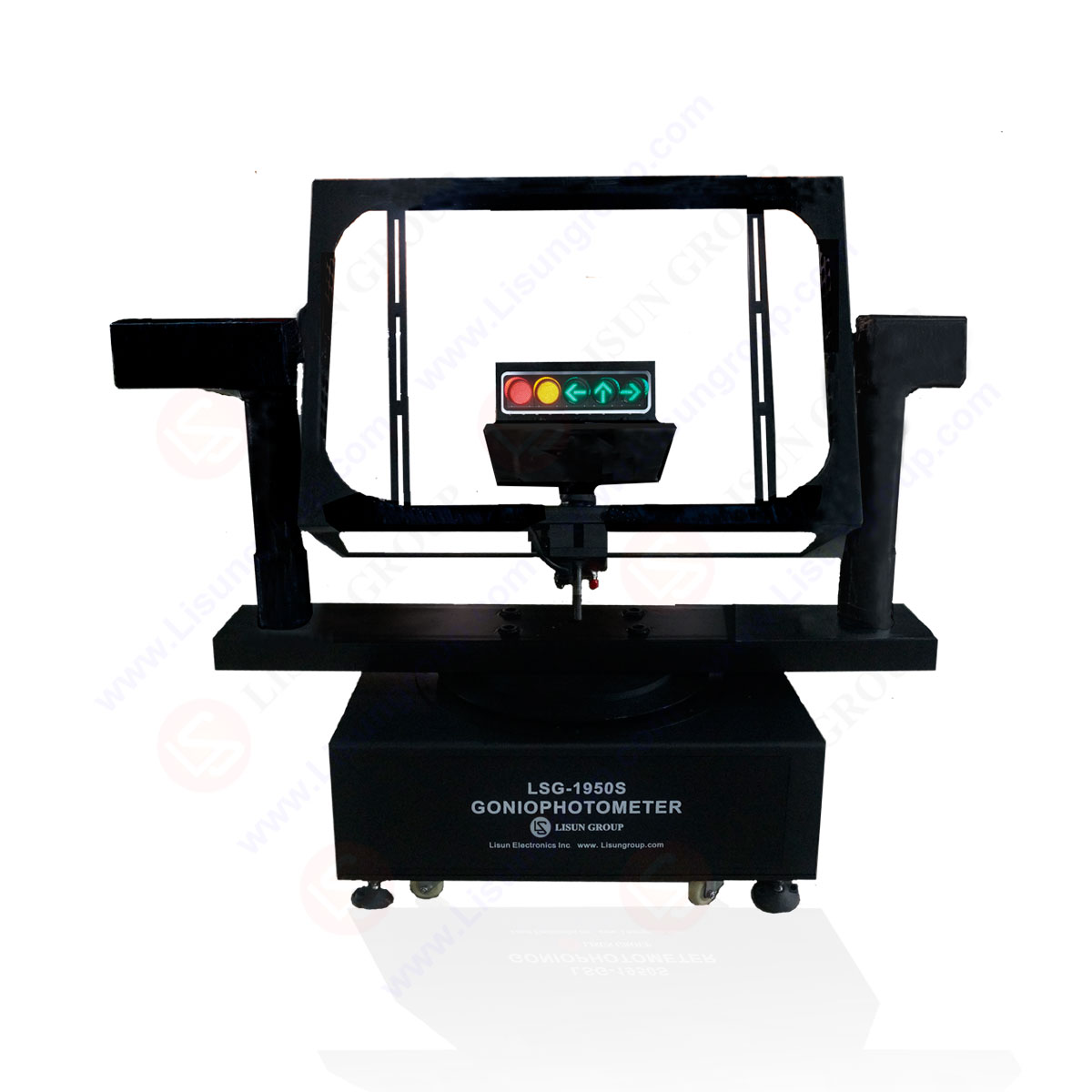
Goniophotometer for Traffic Signal Lamps
LSG-1950S
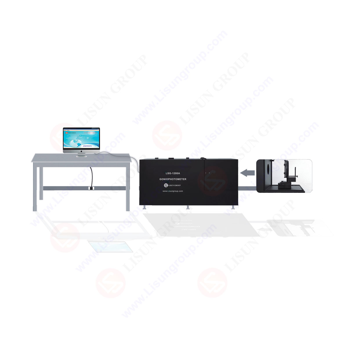
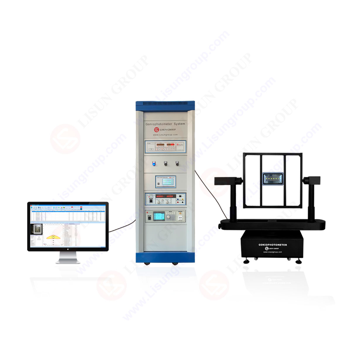
Compact Goniophotometer
LSG-1200A

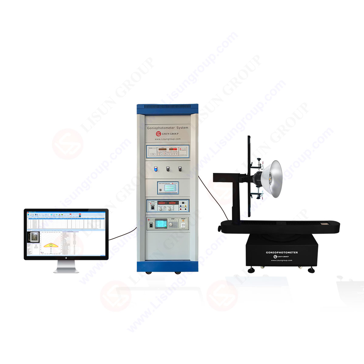
Near Field Moving Detector Goniophotometer
LSG-1900B
Select an organization
to browse standards
Introduction
The semiconductor sector is crucial to the operation of today’s technological marvels, since semiconductor chips are the backbone of all electronic gadgets and infrastructure. The problem of electromagnetic interference (EMI) is becoming more pressing as semiconductor devices get smaller and more complicated.
Electromagnetic interference (EMI) is harmful to electronics and may cause signal deterioration, data corruption, and even system failure in semiconductor chips. This article will discuss electromagnetic interference (EMI) testing and its usefulness in the semiconductor industry for evaluating and reducing electromagnetic interference prior to chip design.
Implementing severe EMI testing procedures allows semiconductor makers to safeguard chip designs, boost product quality, and conform to the demanding standards of today’s electronic gadgets.
The Need for EMI Testing in the Semiconductor Industry
The semiconductor industry is faced with unique electromagnetic interference (EMI) challenges as a result of the high-density integration of electrical components on a single chip. In the business of semiconductors, EMI testing is very significant for a variety of reasons, some of the most important of which are as follows:
Signal Integrity and Performance: Semiconductor chips are able to perform processing and transmission of electronic signals with a high degree of accuracy and efficacy. Signal degradation brought on by electromagnetic interference (EMI) might result in data corruption or other problems. When firms designing semiconductors put their chips through electromagnetic interference (EMI) testing during the design phase, they have a better chance of avoiding problems with functionality and performance that are brought on by interference.
Compliance with Regulatory Standards: The semiconductor industry is required to comply with a multitude of rules, standards, and certifications in order to prevent electromagnetic interference (EMI). Conformity ensures that electronic components will not violate electromagnetic compatibility guidelines or interfere with the operation of other electronic systems. Chip designs are checked for compliance with these criteria by EMI testing, which enables manufacturers to meet the requirements of the legislation and join the market.
Prevention of Crosstalk: On a single semiconductor chip, it is not uncommon to have many separate functional blocks located in close proximity to one another. Interference and a decrease in system performance may result from unwanted signal coupling between these blocks. This phenomenon is referred to as crosstalk. By doing electromagnetic interference (EMI) testing, semiconductor designers may uncover parts of their designs in which crosstalk may occur. They may then make improvements to lessen the risk of interference, such as improving shielding, routing, and isolation.
EMI Resilience in Harsh Environments: Numerous pieces of electronic equipment that use semiconductor chips are susceptible to electromagnetic noise and disturbances when they are placed in harsh environments. In the fields of automobile manufacturing, aeronautical engineering, and industrial automation, companies simply cannot afford for their semiconductor equipment to fail owing to electromagnetic interference (EMI). With the use of EMI testing, manufacturers are able to check the resistance of their chips to external electromagnetic sources and ensure that their products will work consistently.
The Role of EMI Testing in Chip Design
When it comes to the design of chips, electromagnetic interference (EMI) testing is very necessary for locating, comprehending, and minimizing electromagnetic interference. Testing for electromagnetic interference (EMI) in the semiconductor industry consists of the following components:
Pre-compliance Testing: Pre-compliance testing makes use of EMI measurements and assessments to find likely interference sources and quantify the influence on nearby components. This testing takes place throughout the process of chip design. By doing EMI testing before the chip enters the final phase of production, the risk of having to make time-consuming and financially burdensome changes to the design may be reduced. When doing pre-compliance testing, it is common practice to employ specialized EMI test equipment in an anechoic chamber or other environment that is insulated.
Simulation and Modeling: The use of EMI simulation and modeling tools allows for the prediction and investigation of potential EMI issues that may arise in the design of chips. Using sophisticated software tools, designers may assess the electromagnetic interference (EMI) performance of their chip designs by simulating electromagnetic fields, currents, and voltages. Designers can do this by modeling electromagnetic fields with their chip designs. It is typical practice to use simulation in order to determine the likely interference sources and to make targeted design alterations in order to mitigate EMI dangers.
Electromagnetic Shielding: EMI testing is a method that may be used to evaluate how well electromagnetic shielding measures are used in chip designs. Electromagnetic radiation is confined and inhibited within the chip using shielding technologies like metal layers and ground planes. EMI testing guarantees that these techniques of shielding are effective by determining the number of electromagnetic emissions present and determining whether or not they comply with the standards set out by the industry. It assists in the discovery of any spots of failure or inadequate shielding, enabling designers to fine-tune their procedures and guaranteeing total electromagnetic confinement.
Component Placement and Routing: The manner in which components are routed and arranged on a semiconductor chip may have a significant impact on the degree to which it is susceptible to electromagnetic interference (EMI). The major objective of the EMI testing is to determine how the placement of components, signal lines, and power distribution networks influence the electromagnetic compatibility of the chip. Finding potential hotspots for signal coupling, crosstalk, or radiation is the first step in any effort to optimize an electronic system’s design or routing in order to lower the risk of electromagnetic interference (EMI).
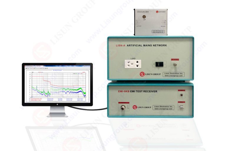
Noise Immunity and Filtering: The purpose of electromagnetic interference (EMI) testing is to measure the efficiency of various filtering methods and the noise immunity of semiconductor chips. Chip vulnerabilities may be identified and suitable filtering mechanisms can be implemented to limit the impacts of external electromagnetic disturbances by testing the chip’s reaction to a variety of noise sources. You can get the best EMI test receivers from LISUN.
Validation of EMI Countermeasures: Multiple preventative steps are used during chip design to lower EMI potential. Among these safeguards are decoupling capacitors, ferrite beads, and electromagnetic interference (EMI) filters. EMI testing verifies the efficiency of these safeguards by monitoring the chip’s operation when electromagnetic interference is present. It verifies that the enacted measures successfully reduce EMI while keeping the chip operational and dependable.
Compliance with EMC Standards: The interoperability and cohabitation of electronic devices relies on the semiconductor industry’s adherence to established electromagnetic compatibility (EMC) standards. Standards from organizations like the International Electrotechnical Commission (IEC) and the Federal Communications Commission (FCC) rely heavily on electromagnetic interference (EMI) testing to ensure that products are compliant. The dependability and compatibility of semiconductors are ensured by rigorous EMI testing, which shows that the chips are within acceptable emission limits and immunity thresholds.
Conclusion
In the semiconductor industry, EMI testing is a crucial part of the chip design process. Manufacturers of semiconductors may guarantee the chips’ performance, dependability, and functioning by analyzing and reducing electromagnetic interference. To reduce the likelihood of electromagnetic interference (EMI), testing may help designers pinpoint the origins of the problem, assess its severity, and apply appropriate mitigation strategies.
Optimizing signal integrity, meeting regulatory requirements, and increasing chips’ robustness under challenging conditions are all areas where it plays a crucial role. EMI testing allows semiconductor makers to produce high-quality chips that fulfill the demanding requirements of modern electronic devices via the use of sophisticated modeling methods, electromagnetic shielding, noise filtering, and smart component placement.
To ensure faultless and reliable performance of semiconductor chips in an increasingly networked and electromagnetic environment, rigorous EMI testing will only increase in relevance as the semiconductor industry continues to expand and innovate.
Lisun Instruments Limited was found by LISUN GROUP in 2003. LISUN quality system has been strictly certified by ISO9001:2015. As a CIE Membership, LISUN products are designed based on CIE, IEC and other international or national standards. All products passed CE certificate and authenticated by the third party lab.
Our main products are Goniophotometer, Integrating Sphere, Spectroradiometer, Surge Generator, ESD Simulator Guns, EMI Receiver, EMC Test Equipment, Electrical Safety Tester, Environmental Chamber, Temperature Chamber, Climate Chamber, Thermal Chamber, Salt Spray Test, Dust Test Chamber, Waterproof Test, RoHS Test (EDXRF), Glow Wire Test and Needle Flame Test.
Please feel free to contact us if you need any support.
Tech Dep: Service@Lisungroup.com, Cell/WhatsApp:+8615317907381
Sales Dep: Sales@Lisungroup.com, Cell/WhatsApp:+8618117273997

LISUN’s Motor-Operated Tool | Power Tool Testing solutions strictly comply with a range of core international standards, providing full support for safety and electromagnetic compatibility (EMC)...
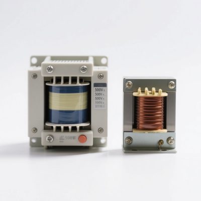
LISUN’s transformer test solutions meet IEC 61558-1, IEC 60076-1, IEC 62041 standards. Covering safety, performance, EMC tests, ensuring transformers comply with global requirements.
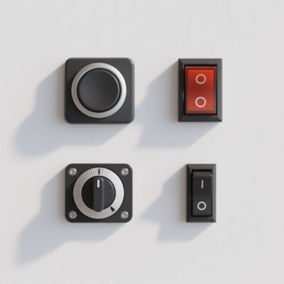
LISUN’s household and appliance switch testing solutions meet IEC 60669, IEC 61058, IEC 62271 standards. Covering electrical, mechanical & EMC tests for global compliance.

For the CFL design and manufactory, LISUN can supply a full quality control test solution, including photometric, colorimetric, electricity, flicker, IES candela distribution, surge test, electrical...

 中文简体
中文简体