LM-79 Moving Detector Goniophotometer (Mirror Type C)
LSG-6000
High Precision Rotation Luminaire Goniophotometer
LSG-1890B
High Precision Rotation Luminaire Goniospectroradiometer
LSG-1890BCCD
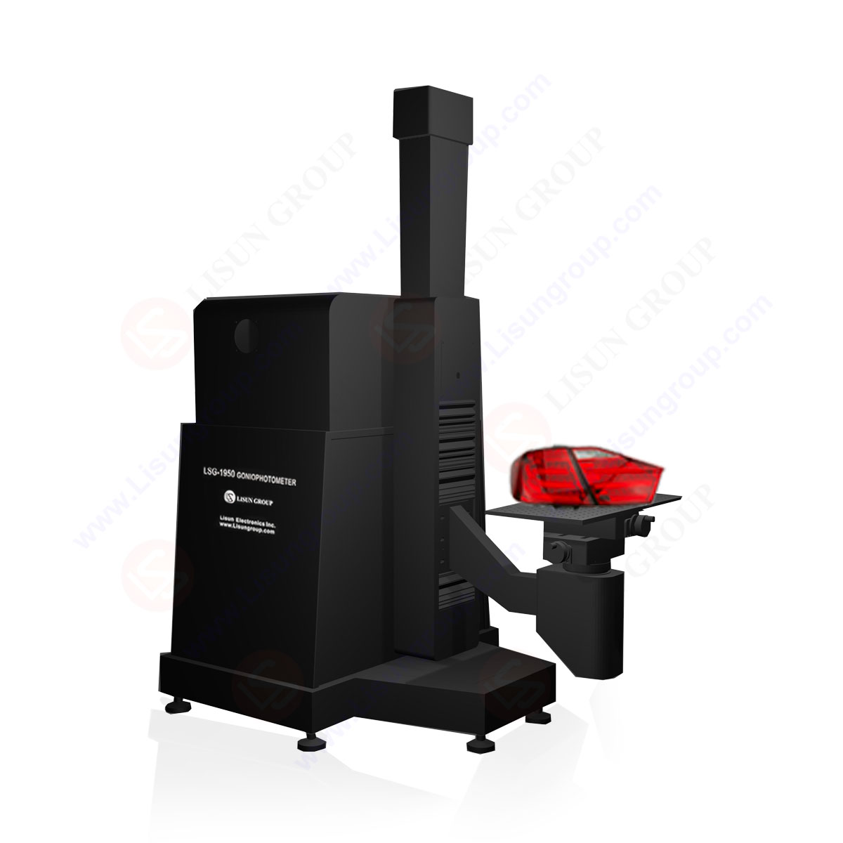
Goniophotometer for Automotive and Signal Lamps
LSG-1950
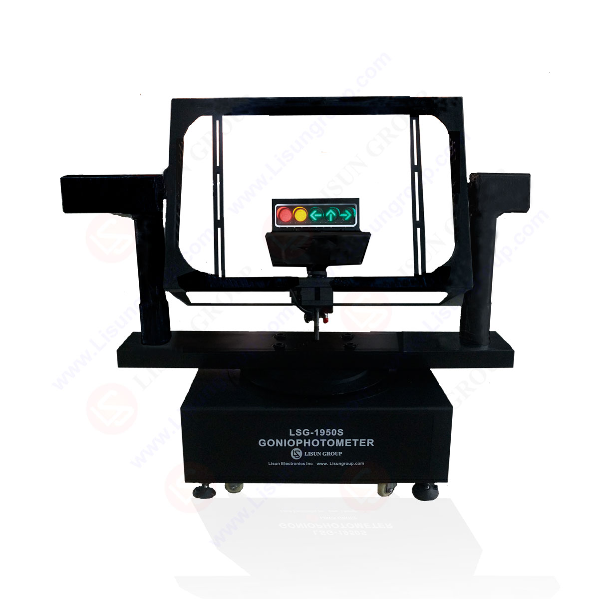
Goniophotometer for Traffic Signal Lamps
LSG-1950S
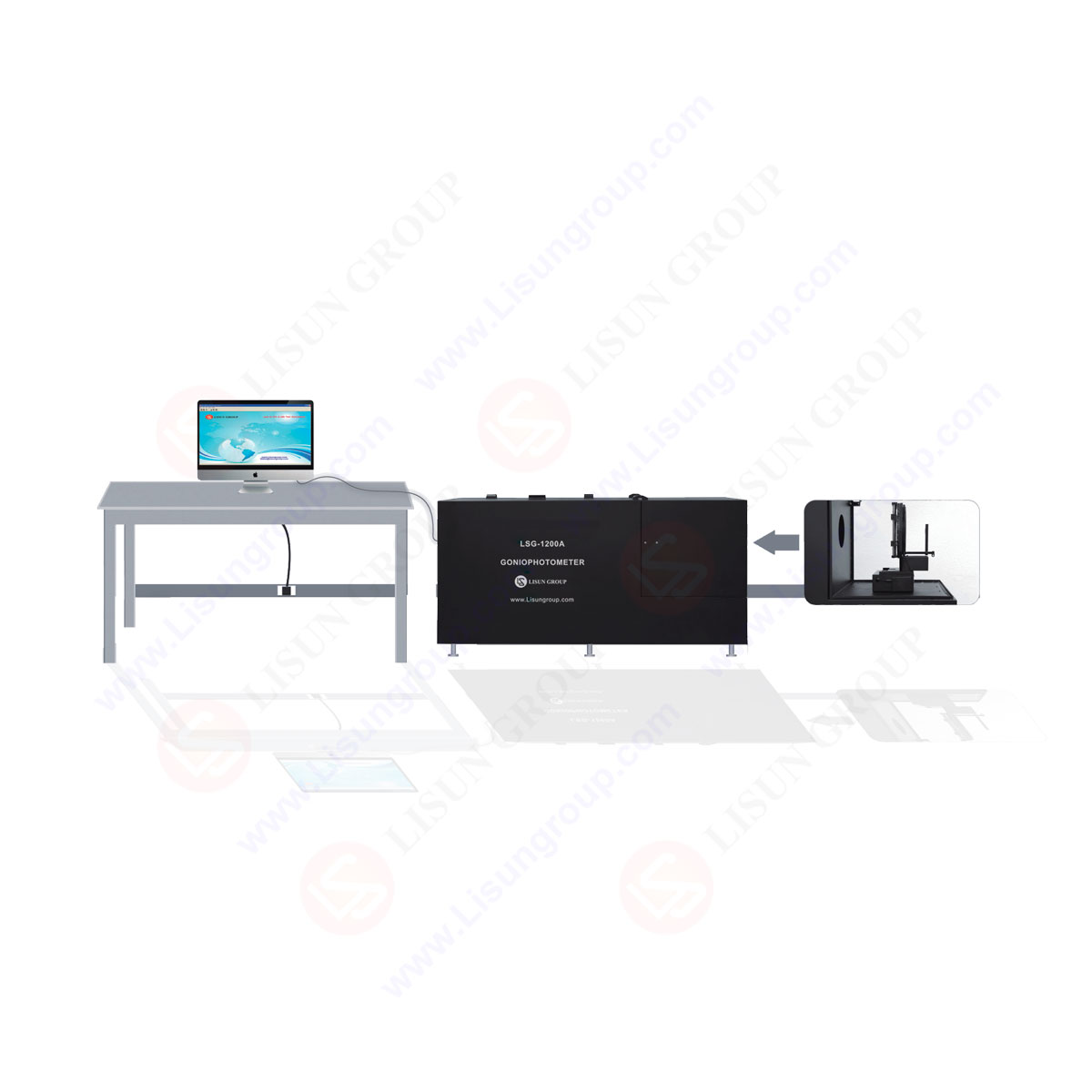
Compact Goniophotometer
LSG-1200A

Near Field Moving Detector Goniophotometer
LSG-1900B
Select an organization
to browse standards
Abstract
Against the backdrop of the rapid development of the semiconductor industry, the problem of damage to semiconductor devices caused by electrostatic discharge (ESD) has become increasingly prominent. The Human Body Model (HBM) and Machine Model (MM) are the main sources of electrostatic threats faced by semiconductor devices during production, transportation, and use. This article focuses on the LISUN ESD-883D Electrostatic Discharge Simulator (HBM/MM), elaborating in detail on its design principles, compliance with international and domestic standards, equipment features, specifications, and applications in ESD susceptibility testing of semiconductor devices such as LED chips, transistors, and ICs. Through a comprehensive analysis of this equipment, this article demonstrates its important role in ensuring the quality and reliability of semiconductor devices, providing a reference for relevant testing work in the semiconductor industry.
1. Introduction
As semiconductor technology continues to move towards miniaturization and high integration, the sensitivity of semiconductor devices to static electricity has increased significantly. Electrostatic discharge (ESD), as a common electromagnetic interference phenomenon, may cause semiconductor devices to suffer from performance degradation, functional failure, or even permanent damage, bringing huge economic losses to the semiconductor industry. According to relevant statistical data, ESD-induced failures account for more than 25% of the failure cases of semiconductor devices, making it a key factor affecting the reliability of semiconductor devices.
The Human Body Model (HBM) simulates the electrostatic discharge process that occurs when a charged human body comes into contact with semiconductor devices, while the Machine Model (MM) simulates the electrostatic discharge between production equipment, automated machinery, and other devices and semiconductor devices during operation. If the electrostatic energy generated by these two discharge models exceeds the tolerance limit of semiconductor devices, it will cause serious damage to the devices. Therefore, ESD susceptibility testing of semiconductor devices based on HBM and MM has become an indispensable step in the production, R&D, and quality inspection of semiconductor devices.
As a professional manufacturer of testing equipment, LISUN GROUP has developed and launched the ESD-883D Electrostatic Discharge Simulator (HBM/MM) in response to the characteristics and testing requirements of HBM and MM. This equipment can accurately simulate the electrostatic discharge processes of HBM and MM, and conduct ESD susceptibility testing on semiconductor devices in accordance with relevant international and domestic standards. It provides a reliable testing method for quality control of semiconductor devices and has been widely used in the semiconductor industry.
: A Core Equipment for ESD Susceptibility Testing of Semiconductor Devices 3")
ESD-883D
2. Principles of HBM and MM Discharge Models and Significance of Testing
2.1 Principle of Human Body Model (HBM)
The Human Body Model (HBM) is established based on the physical process where a human body accumulates static electricity due to friction and other factors during daily activities, and the static electricity is discharged through the semiconductor device when the human body comes into contact with it. In the HBM model, the human body can be regarded as an equivalent circuit composed of a capacitor and a resistor. Generally, the equivalent capacitance of the HBM model is approximately 100pF, and the equivalent resistance is about 1500Ω. This parameter configuration can relatively accurately simulate the actual situation of electrostatic discharge when a charged human body comes into contact with a semiconductor device. When a human body carrying static charge comes into contact with a semiconductor device, the charge will be quickly released through the device, forming an instantaneous large current. This current will generate an excessively high voltage drop inside the semiconductor device, which may break down the insulating layer of the device, damage the PN junction, and eventually lead to device failure.
2.2 Principle of Machine Model (MM)
The Machine Model (MM) mainly simulates the electrostatic discharge process that occurs between automated equipment, robotic arms, conveyor belts, and other machinery on the production line and semiconductor devices after the machinery accumulates static electricity due to friction, induction, and other effects during operation. Compared with HBM, MM has a larger equivalent capacitance (usually 200pF) and a smaller equivalent resistance (close to 0Ω). This makes the current rise rate of the MM discharge process faster, the peak current larger, and the released electrostatic energy stronger, resulting in more significant damage to semiconductor devices. In the automated production process of semiconductor devices, ESD accidents caused by MM often lead to batch damage of devices. Therefore, ESD susceptibility testing based on MM is particularly important.
2.3 Significance of HBM and MM ESD Susceptibility Testing
Conducting HBM and MM ESD susceptibility testing on semiconductor devices is of great significance in multiple aspects. From the perspective of device R&D, testing can accurately help understand the tolerance of devices under different electrostatic discharge models, providing data support for device structure design, material selection, and process optimization, and contributing to the development of semiconductor devices with better electrostatic protection capabilities. In the production process, testing can screen the quality of produced semiconductor devices, eliminate products that do not meet requirements due to high electrostatic sensitivity, ensure the quality stability of delivered devices, and reduce the risk of device failure caused by static electricity for downstream enterprises. For downstream application enterprises, conducting ESD susceptibility testing on purchased semiconductor devices can verify whether the devices meet the usage requirements of their own products, ensure the reliability of end products during production and use, and avoid faults in end products caused by ESD failure of semiconductor devices.
3. Standards Complied with by LISUN ESD-883D Electrostatic Discharge Simulator (HBM/MM)
During the design and manufacturing process, the LISUN ESD-883D Electrostatic Discharge Simulator (HBM/MM) strictly adheres to a number of international and domestic standards, ensuring the accuracy, reliability, and universality of its testing results, and can meet the ESD susceptibility testing requirements of semiconductor devices in different countries, regions, and industries.
The above standards specify in detail the test conditions, test procedures, parameter requirements, and result determination of HBM and MM electrostatic discharge testing. The LISUN ESD-883D Electrostatic Discharge Simulator (HBM/MM) not only fully meets the requirements of these standards but also can satisfy the most severe electrostatic voltage requirements in each standard, ensuring that it can provide accurate and effective ESD susceptibility testing for semiconductor devices in various harsh testing scenarios. For example, in the HBM testing standards, some standards require a maximum electrostatic voltage of 8kV, and the output voltage range of this equipment in HBM mode is 0.1~8kV±5%, which can accurately cover this strict voltage requirement; in the MM testing standards, the maximum electrostatic voltage requirement is 800V, and the output voltage range of the equipment in MM mode (100~800V±5%) also fully meets the testing needs.
4. Features of LISUN ESD-883D Electrostatic Discharge Simulator (HBM/MM)
The LISUN ESD-883D Electrostatic Discharge Simulator (HBM/MM) fully considers the practicality, stability, and safety of testing work in its design, and has many outstanding features, providing high-quality equipment support for ESD susceptibility testing of semiconductor devices.
4.1 User – Friendly Operation Interface
The equipment is equipped with a color touch LCD interface, which has a concise and intuitive design and clear operation logic. Testers can quickly master the operation method of the equipment without going through complex training. Through the touch screen, testers can easily set test parameters such as output voltage, discharge polarity, number of discharges, and discharge interval; at the same time, the screen can display key parameters during the test process in real – time, such as the current discharge voltage, number of discharges, and working status of the equipment, which is convenient for testers to monitor the test process in real – time and promptly detect and handle problems that occur during the test.
4.2 High – Precision and Stable Output Performance
Output voltage accuracy is one of the key indicators to measure the performance of an electrostatic discharge simulator, which directly affects the accuracy of test results. The LISUN ESD-883D Electrostatic Discharge Simulator (HBM/MM) adopts advanced voltage control technology, with an output voltage accuracy of ±5% in both HBM mode and MM mode. This ensures that the voltage value of each discharge accurately meets the requirements of the test standard and avoids test result errors caused by voltage deviations. In addition, the equipment uses high – quality electronic components and a stable circuit design inside, which effectively reduces the impact of external factors (such as power grid voltage fluctuations, environmental temperature changes, etc.) on the output performance, ensuring the output stability of the equipment during long – term continuous testing and providing a strong guarantee for the reliability of the testing work.
4.3 Comprehensive Safety Protection Mechanism
High – voltage electricity is involved in the electrostatic discharge testing process, so the safety performance of the equipment is crucial. This equipment is equipped with an intelligent programmable high – voltage power supply and is provided with high – voltage over – voltage, over – current, and short – circuit protection functions. When the equipment detects that the high – voltage output exceeds the set safety threshold, the output current is too large, or a short – circuit fault occurs, it will immediately cut off the high – voltage output automatically and issue an alarm signal at the same time, preventing damage to the equipment itself, test samples, and testers due to abnormal high voltage. This comprehensive safety protection mechanism greatly reduces the safety risks during the testing process and provides a solid guarantee for the personal safety of testers and the normal operation of the equipment.
4.4 Intelligent Self – Diagnosis Function
In order to promptly detect potential fault hazards of the equipment and ensure that the equipment is always in a good working state, the LISUN ESD-883D Electrostatic Discharge Simulator (HBM/MM) is equipped with a self – diagnosis function. When the equipment is started and during the test process, it will automatically detect the internal key components (such as high – voltage power supply, control circuit, discharge circuit, etc.). If an abnormal component or unstable working state is detected, the equipment will display fault information through the LCD interface, prompting testers to carry out maintenance and repair in a timely manner. Through the self – diagnosis function, the time for equipment fault diagnosis can be effectively shortened, the maintenance efficiency of the equipment can be improved, the interruption of the testing work caused by equipment faults can be reduced, and the smooth progress of the testing work can be ensured.
4.5 High Cost – Effectiveness Advantage
On the premise of ensuring the performance and quality of the equipment, the LISUN ESD-883D Electrostatic Discharge Simulator (HBM/MM) also has a high cost – effectiveness. The main components of the equipment are all imported high – quality components, which have the advantages of high precision, strong reliability, and long service life. These components can effectively reduce the failure rate of the equipment and reduce the later maintenance cost of the equipment. At the same time, LISUN GROUP controls the production cost of the equipment by optimizing the production process and improving production efficiency, while providing users with products with excellent performance and reasonable prices. This makes the equipment have strong competitiveness in the market and can meet the testing needs of semiconductor enterprises of different scales. Whether it is a small R&D laboratory or a large – scale production enterprise, high – quality electrostatic susceptibility testing can be realized through this equipment.
: A Core Equipment for ESD Susceptibility Testing of Semiconductor Devices - LISUN")
5. Specifications of LISUN ESD-883D Electrostatic Discharge Simulator (HBM/MM)
Specifications are an important basis for understanding the performance and application scope of the equipment. The detailed specifications of the LISUN ESD-883D Electrostatic Discharge Simulator (HBM/MM) are shown in the following table:
| Parameter Category | Specific Parameter | Human Body Discharge Mode (HBM) | Machine Discharge Mode (MM) |
| Output Voltage | Range | 0.1~8kV | 100~800V |
| Accuracy | ±5% | ±5% | |
| Output Polarity | – | Positive, Negative, Alternating Positive and Negative | Positive, Negative, Alternating Positive and Negative |
| Trigger Mode | – | Single, Count, Host Self – Trigger | Single, Count, Host Self – Trigger |
| Single Trigger | Single Discharge | Single Discharge | |
| Count Trigger | Discharge According to the Set Number of Discharges | Discharge According to the Set Number of Discharges | |
| Discharge Mode | – | Human Body Model (HBM) | Machine Model (MM) |
| Discharge Interval | – | 1~99s | 1~99s |
| Number of Discharges | – | 1~999 Times | 1~999 Times |
| Discharge Capacitance | – | 100pF±10% | 200pF±10% |
| Discharge Resistance | – | 1500Ω±10% | 0Ω±10% |
| System Power Supply | – | AC 100~240V, 50/60Hz, 300W | AC 100~240V, 50/60Hz, 300W |
| Operating Environment | Temperature | 15°C~35°C | 15°C~35°C |
| Humidity | 10%~75% | 10%~75% |
It can be seen from the above specifications that the equipment has high flexibility in the setting of discharge parameters. It can adjust parameters such as output voltage, discharge polarity, number of discharges, and discharge interval according to the testing requirements of different semiconductor devices and different standards, meeting diversified testing scenarios. For example, when testing LED chips with different sensitivities, testers can select an appropriate output voltage in HBM mode according to the specifications of the chips (for chips with low sensitivity, a higher voltage can be selected for testing; for chips with high sensitivity, a lower voltage can be selected), and set the corresponding number of discharges and intervals to fully evaluate the ESD susceptibility performance of the chips.
In addition, the discharge capacitance and discharge resistance parameters of the equipment are designed in strict accordance with the standard requirements of HBM and MM. The 100pF±10% discharge capacitance and 1500Ω±10% discharge resistance in HBM mode, as well as the 200pF±10% discharge capacitance and 0Ω±10% discharge resistance in MM mode, can accurately simulate the electrostatic discharge characteristics of the two discharge models, ensuring that the test results have high accuracy and reference value. At the same time, the wide – range system power input (AC 100~240V) of the equipment enables it to work normally in the power grid environments of different countries and regions, enhancing the universality of the equipment; the temperature range of 15°C~35°C and the humidity range of 10%~75% also meet the environmental conditions of most semiconductor testing laboratories, facilitating the installation and use of the equipment.
It is worth noting that the LISUN ESD-883D Electrostatic Discharge Simulator (HBM/MM) also has good expandability. It can share a host with the ESD – CDM Charged Device Model (CDM) Semiconductor Electrostatic Discharge Simulator to form a comprehensive testing system (model: ESD – 883D/ESD – CDM) that can test three discharge models (HBM, MM, and CDM) at the same time. This design not only saves the purchase cost of the equipment and the space occupied by the laboratory but also provides convenience for users to carry out CDM electrostatic susceptibility testing in the future, further improving the cost – effectiveness and use value of the equipment.
6. Applications of LISUN ESD-883D Electrostatic Discharge Simulator (HBM/MM) in Semiconductor Device Testing
With its excellent performance and flexible configuration, the LISUN ESD-883D Electrostatic Discharge Simulator (HBM/MM) has been widely used in the ESD susceptibility testing of various semiconductor devices such as LED chips, transistors, and ICs, providing strong support for the quality control and reliability improvement of semiconductor devices.
6.1 Application in LED Chip Testing
As the core device in the fields of semiconductor lighting and display, the performance and reliability of LED chips directly affect the quality of end – products. During the production process of LED chips, from wafer manufacturing, chip cutting to packaging testing, they may face the threat of electrostatic discharge. The LISUN ESD-883D Electrostatic Discharge Simulator (HBM/MM) can conduct HBM and MM ESD susceptibility testing on LED chips in accordance with relevant standards.
During the test, the LED chip is fixed on a special test fixture. According to the test standard and the specifications of the chip, an appropriate output voltage (such as 1kV, 2kV, 5kV, 8kV, etc.) and number of discharges are set in HBM mode, and then the equipment is started for discharge testing. After the test is completed, the photoelectric parameters of the LED chip (such as luminous intensity, luminous flux, forward voltage, reverse leakage current, etc.) are detected to judge the performance change of the chip under HBM electrostatic discharge. If there is no obvious change in the photoelectric parameters of the chip, it indicates that it can withstand the HBM electrostatic discharge of this voltage level; if the parameters are significantly degraded or the chip cannot emit light normally, it indicates that the HBM ESD susceptibility of the chip does not meet the requirements.
Similarly, in MM mode, different output voltages such as 100V, 300V, 500V, and 800V are set according to the test requirements to conduct electrostatic discharge testing on the LED chip and detect the performance of the chip. Through this testing method, LED chips with high electrostatic sensitivity can be effectively screened out, preventing unqualified products from flowing into the downstream packaging link, thereby ensuring the reliability and service life of end – products such as LED lamps and display screens.
6.2 Application in Transistor Testing
As the basic switching and amplifying components in electronic circuits, transistors are widely used in computers, communication equipment, consumer electronics, and other fields. The structure of transistors is precise, and key parts such as PN junctions are extremely sensitive to electrostatic discharge. Once they are subjected to electrostatic shock, faults such as PN junction breakdown and base open circuit may occur, making the transistors lose their normal functions. Therefore, it is crucial to conduct HBM and MM ESD susceptibility testing on transistors.
When using the LISUN ESD-883D Electrostatic Discharge Simulator (HBM/MM) to test transistors, appropriate test pins (such as base, emitter, collector) should be selected for discharge according to the type of transistor (such as NPN type, PNP type, MOSFET, etc.) and the test standard. For example, when testing an NPN – type transistor in HBM mode, the discharge electrode is usually connected to the base of the transistor, the emitter and collector are grounded, and then the corresponding output voltage and number of discharges are set for testing. After the test is completed, a transistor characteristic tester is used to detect the parameters of the transistor, such as current gain (β), reverse breakdown voltage (BVCEO, BVCBO, etc.), and leakage current (ICBO, IEBO, etc.), to evaluate the performance of the transistor after electrostatic discharge.
For field – effect transistors such as MOSFETs, due to their very thin gate oxide layer, they are more sensitive to static electricity. Therefore, more care should be taken in selecting the test voltage and discharge method during testing. The high – precision voltage control and stable discharge performance of the LISUN ESD – 883D can ensure accurate control of the discharge energy during the test, avoid additional damage to the MOSFET caused by improper test operations, and accurately evaluate its ESD susceptibility performance. By conducting comprehensive HBM and MM ESD susceptibility testing on transistors, the quality stability of transistor products can be improved, and the failure of electronic equipment caused by electrostatic discharge can be reduced.
6.3 Application in IC Testing
Integrated circuits (ICs) are the core products of the semiconductor industry, with the characteristics of high integration, complex functions, and precise internal structure. They contain a large number of components such as transistors, resistors, and capacitors. If any component is damaged by electrostatic discharge, the entire IC chip may fail to function. Therefore, the ESD susceptibility testing of IC chips is a key link in their quality inspection.
The LISUN ESD-883D Electrostatic Discharge Simulator (HBM/MM) can conduct HBM and MM ESD susceptibility testing on various IC chips (such as microprocessors, memories, sensors, power management ICs, etc.) in accordance with standards such as AEC – Q100 – 002, AEC – Q100 – 003, and MIL – STD – 883 Method 3015. Before the test, a detailed test plan needs to be formulated according to the pin definition of the IC chip and the test standard, and the pins (such as power pins, signal pins, ground pins, etc.) that need to be subjected to discharge testing and the corresponding discharge voltage levels are determined.
During the test, the IC chip is installed on a test socket that meets the standard, and a special discharge probe is used to contact the specified pins for electrostatic discharge according to the set parameters. After the test is completed, an IC test system is used to conduct a comprehensive test on various functions of the IC chip, such as logic function test, timing test, and electrical parameter test, to judge whether the IC chip can work normally after electrostatic discharge. For IC chips used in the automotive electronics field, due to their harsher working environment and higher requirements for ESD susceptibility, they usually need to undergo more stringent HBM and MM testing in accordance with the AEC – Q100 standard. The LISUN ESD – 883D can meet these high – standard testing requirements and provide strong support for the quality assurance of automotive electronic IC chips.
Through its applications in the testing of semiconductor devices such as LED chips, transistors, and ICs, the LISUN ESD-883D Electrostatic Discharge Simulator (HBM/MM) helps semiconductor enterprises effectively identify the electrostatic sensitivity problems of devices, optimize product design and production processes, improve the electrostatic protection capabilities of products, reduce the failure risk of products in market applications, and promote the high – quality development of the semiconductor industry.
7. Conclusions and Prospects
7.1 Conclusions
As a testing equipment specially designed for the Human Body Model (HBM) and Machine Model (MM), the LISUN ESD-883D Electrostatic Discharge Simulator (HBM/MM) has shown excellent performance in the field of ESD susceptibility testing of semiconductor devices. This equipment strictly adheres to a number of international and domestic standards, can meet the most severe electrostatic voltage requirements in different standards, and provides a guarantee for the accuracy and universality of test results. Its user – friendly operation interface, high – precision and stable output performance, comprehensive safety protection mechanism, intelligent self – diagnosis function, and high cost – effectiveness make it an ideal choice for semiconductor enterprises, R&D institutions, and testing laboratories to carry out ESD susceptibility testing.
In practical applications, this equipment can effectively conduct HBM and MM ESD susceptibility testing on various semiconductor devices such as LED chips, transistors, and ICs. It helps relevant enterprises screen unqualified products, optimize product design and production processes, significantly improve the quality and reliability of semiconductor devices, reduce economic losses caused by electrostatic discharge, and is of great significance for promoting the healthy development of the semiconductor industry.
Tags:ESD-883D

 中文简体
中文简体