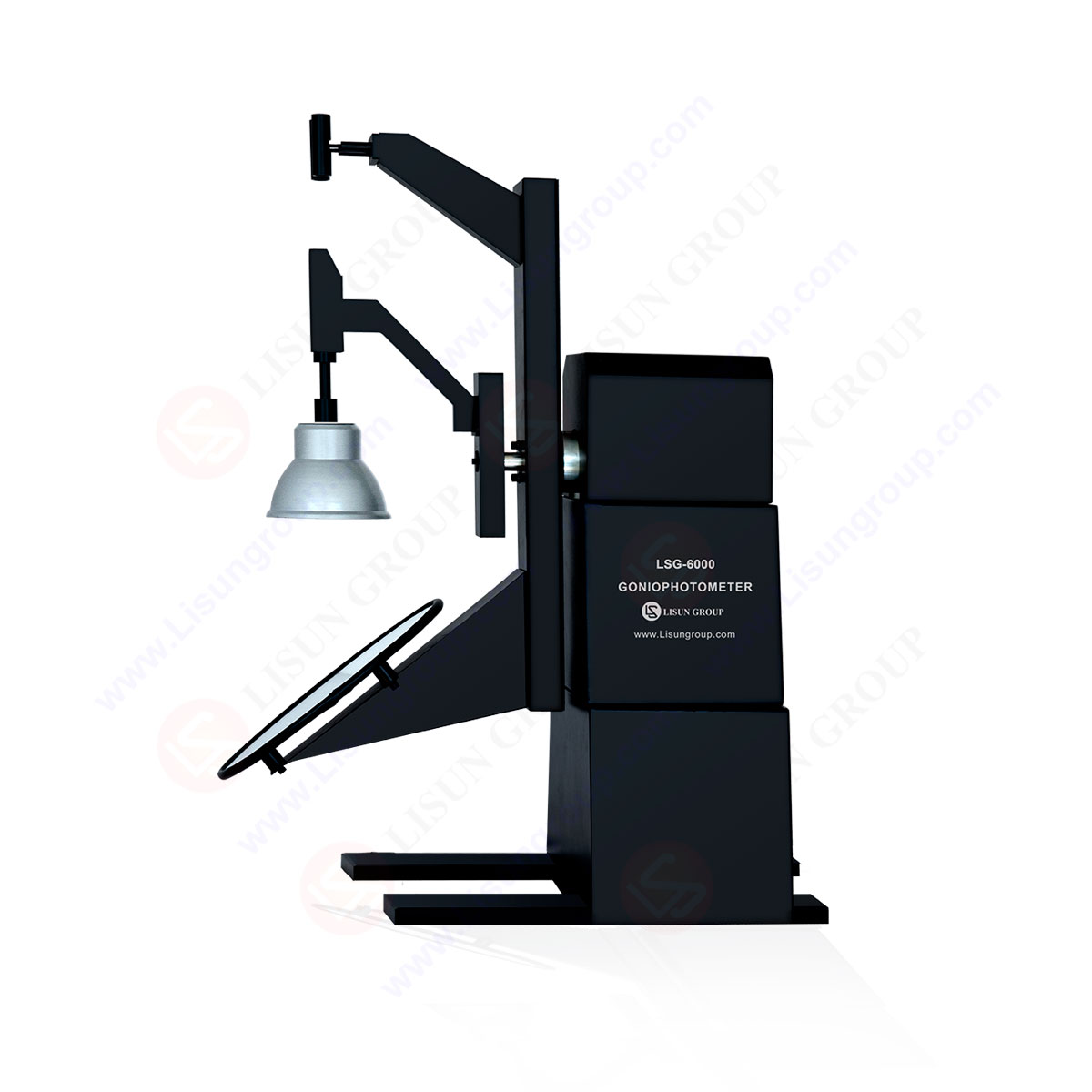
LM-79 Moving Detector Goniophotometer (Mirror Type C)
LSG-6000
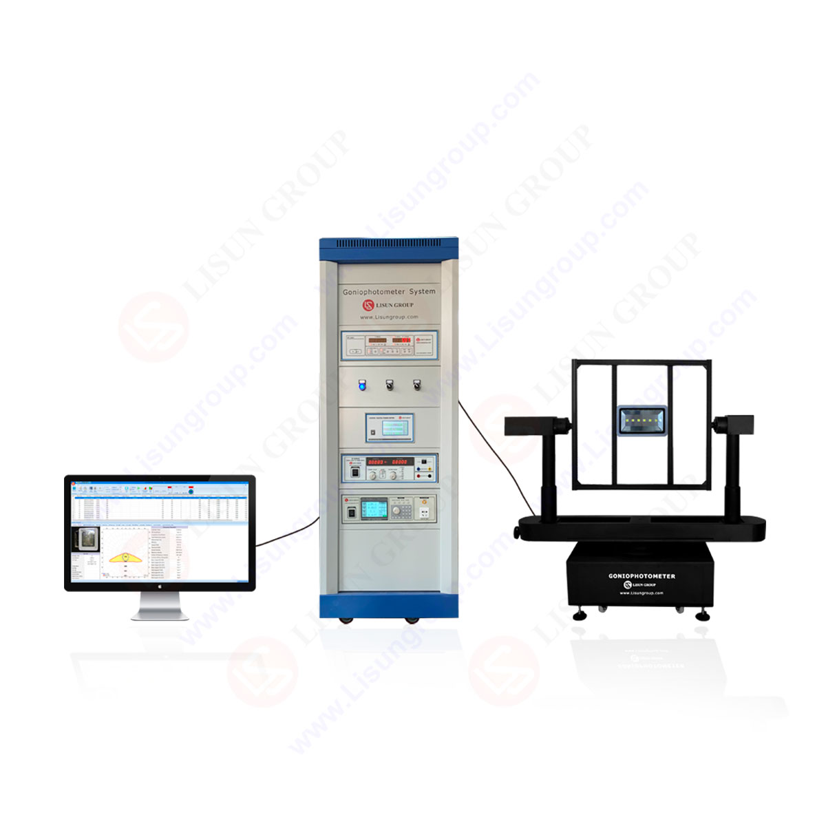
High Precision Rotation Luminaire Goniophotometer
LSG-1890B
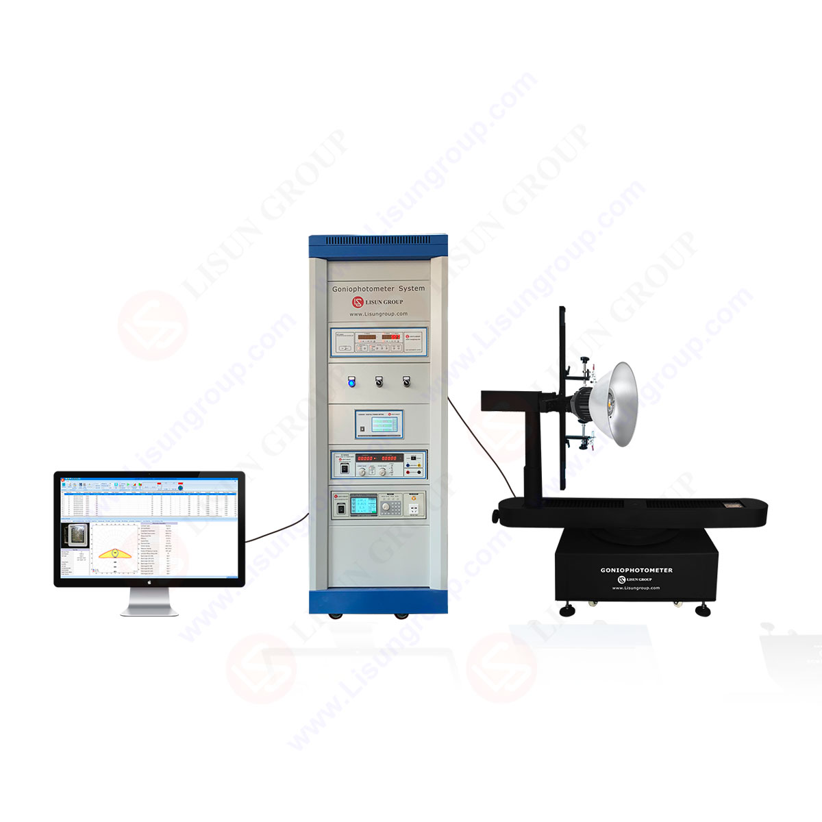
High Precision Rotation Luminaire Goniospectroradiometer
LSG-1890BCCD
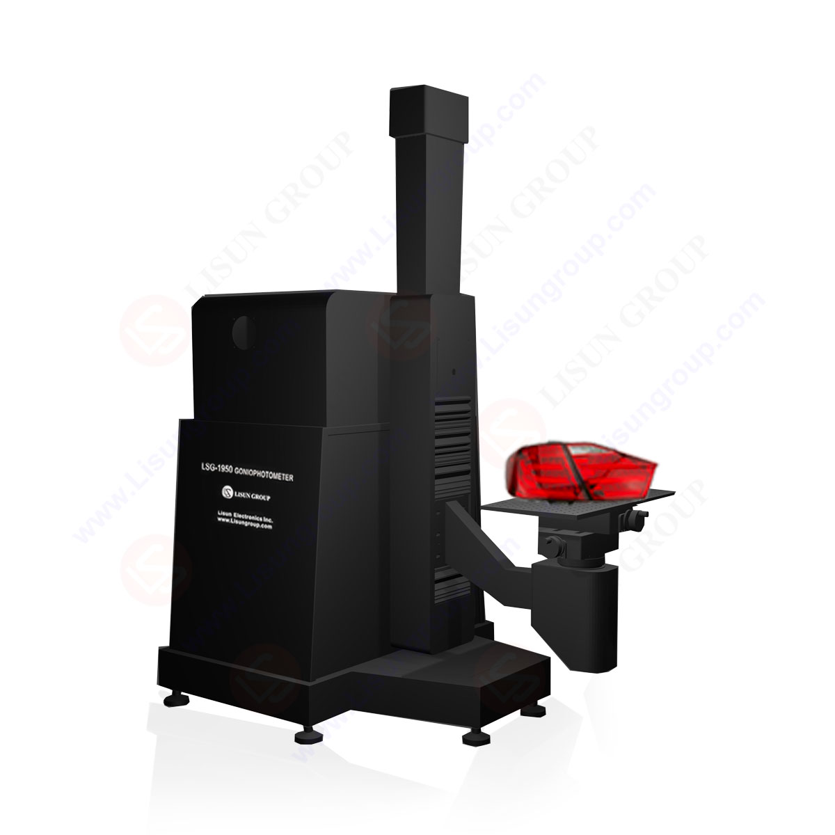
Goniophotometer for Automotive and Signal Lamps
LSG-1950
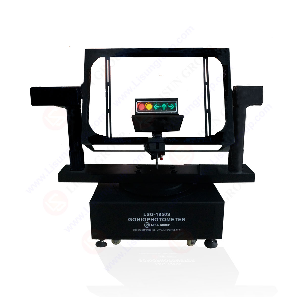
Goniophotometer for Traffic Signal Lamps
LSG-1950S
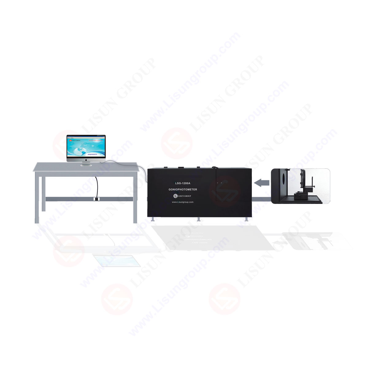
Compact Goniophotometer
LSG-1200A

Near Field Moving Detector Goniophotometer
LSG-1900B
Select an organization
to browse standards
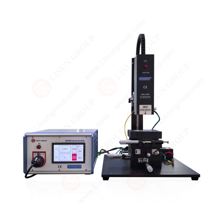
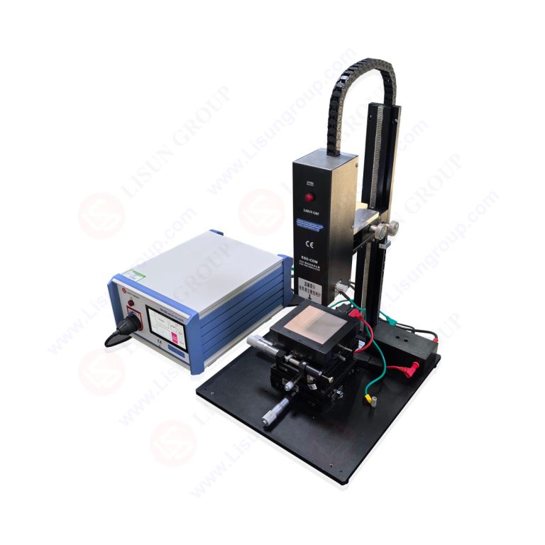


Product No: ESD-CDM
The ESD-CDMCharged Device Model (CDM) ESD Guns for ICs Testing is a high-precision immunity testing device specifically designed by LISUN for the “charged device contact discharge” scenarios of semiconductor components during production, transportation and assembly processes. The function is to simulate the instantaneous discharge process that occurs when a semiconductor component—after becoming charged itself (e.g., via triboelectrification or inductive charging): comes into contact with grounded objects (such as test fixtures, PCB boards, or automated equipment). By precisely controlling parameters like discharge voltage and current waveform, it evaluates the component’s tolerance limit to such “hidden electrostatic shocks,” proactively identifies risks (e.g., internal circuit burnout or functional failure of chips) caused by CDM discharge, and provides critical testing basis for the reliability design, mass-production quality inspection, and international compliance certification of semiconductor components.
The ESD-CDM Charged Device Model (CDM) ESD Guns adopts an innovative integrated structure of “charge injection – contact discharge”, addressing the pain points of traditional CDM testing equipment such as complex operation and poor waveform stability. It is equipped with a high-precision charge measurement module that can real-time monitor the charged quantity of the device, ensuring a discharge voltage error of ≤ ±3%. Combined with customized semiconductor device fixtures (compatible with mainstream packages including DIP, SOP, QFP, and BGA) and a large-sized Android touchscreen supporting both Chinese and English, the ESD-CDM enables one-click configuration of test parameters, automated control of the discharge process, and real-time storage of test data (voltage and current waveforms). This significantly improves the efficiency and data repeatability of semiconductor device ESD testing, meeting the semiconductor industry’s demand for high-precision and high-compatibility testing equipment.
| Discharge Model | International Standards | GB Standards |
| Charged Device Model (CDM) |
ANSI/ESDA/JEDEC JS-002-2014 “Electrostatic Discharge (ESD) Sensitivity Testing -Charged-Device Model (CDM)-Component Level” |
GB/T 4937.28-2024 《半导体器件 机械和气候试验方法 第 28 部分:静电放电敏感度试验 充电器件模型》(等同采用 IEC 60749-28:2022) |
| IEC 60749-28:2022 “Semiconductor devices-Mechanical and climatic test methods -Part 28: Electrostatic discharge (ESD) sensitivity testing-Charged-device model (CDM)” |
||
| AEC-Q100-011 “Charged Device Model (CDM) Electrostatic Discharge Test” | ||
| EIA/JESD22-C101 “Test Method for Electrostatic Discharge Sensitivity Testing -Charged-Device Model (CDM)” |
||
| ANSI/ESD S5.3.1-2009 “Electrostatic Discharge Sensitivity Testing – Charged Device Model (CDM) – Component Level” |
||
| JEITA ED-4701/300 Test Method 305 “Charged Device Model Electrostatic Discharge (CDM/ESD)” |
The ESD-CDM system mainly consists of three parts: DC high voltage source, Main instrument and electrostatic test probe (including attenuator). It can realize the electrostatic induction charging, electrostatic discharge and discharge signal acquisition test functions of the charged device model (CDM). Note: The ESD-CDM can share a host with the ESD-883D HBM/MM ESD Simulators to test HBM, MM and CDM at the same time (LISUN model: ESD-883D/ESD-CDM)
System Configuration:
1. DC high voltage source:
a. Voltage Output Range: ±(10V ~ 5kV)It covers the conventional CDM test voltage requirements of semiconductor devices and is suitable for testing devices with different susceptibility levels (e.g., Class 0 ~ Class 3).
b. Voltage Output Accuracy: ±(3% of reading + 10V)It ensures precise control of the charged voltage and meets the voltage error requirements specified in the IEC 60749-28:2021 standard.
2. Host instrument:
a. Insulation Safety Design: Built-in high-voltage isolation mechanism, which provides insulation and isolation for the high-voltage induction plate to prevent high-voltage leakage, ensuring the safety of operators and equipment.
b. Displacement Adjustment Function: The integrated “high-voltage induction plate + isolation plate” supports X/Y/Z three-axis displacement adjustment. The adjustment range is 0~10cm, and the adjustment accuracy reaches 0.1mm (manual adjustment), enabling precise adaptation to semiconductor devices with different package sizes.
c. Induction Plate Specifications: 12cm×12cm×2mm. It provides a uniform and stable electrostatic induction field, meeting the field strength requirements for device charging in CDM testing.
d. Isolation Plate Specifications: 12cm×12cm×0.4mm. Made of FR4 material, it features both insulation and structural stability, complying with the material requirements for test platforms specified in JEDEC JESD22-C103-J.
3. Electrostatic test probe:
a. Current Measurement Capability: The maximum measurable peak value of electrostatic discharge current pulse is ≥20A. It covers the current monitoring requirements of high-voltage (e.g., 5kV) CDM testing and can accurately capture the peak current at the moment of discharge.
b. Probe Physical Parameters: Diameter Φ1.5mm × Length 10mm, with a telescopic length of approximately 3mm. It is compatible with semiconductor devices of different package heights (e.g., thin SMD, thick TO packages) to ensure precise discharge contact.
c. Movement Control: Supports vertical movement (dual modes: program control + manual control). The movement speed is adjustable from 0.1cm/s to 5cm/s, ensuring stable and controllable discharge contact process.
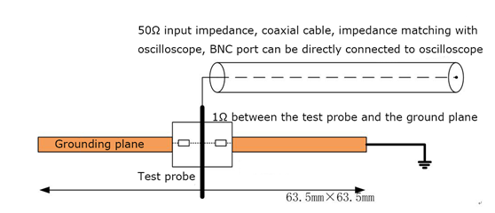
d. Signal Acquisition: Equipped with a dedicated attenuator and reserved data acquisition interfaces/cables. It can be directly connected to an oscilloscope to realize real-time acquisition and analysis of discharge current waveforms.
e. Ground Plate Specifications: 63.5mm × 63.5mm × 6.35mm. It provides a standard ground reference plane to ensure consistency of the testing environment.
Test Methods:
1. IC Device Installation: Place the semiconductor device under test (DUT) on the insulating isolation plate of the test main unit, and fix it with an adaptive fixture. Ensure the device pins face upward and there is no looseness (to prevent displacement during testing from affecting discharge accuracy).
2. Position Calibration: By adjusting the three-dimensional knobs (X/Y/Z axes) of the base, accurately position the target pin of the DUT to the center position directly below the test probe. It is recommended that the calibration accuracy be ≤ 0.1mm (refer to the positioning error requirements specified in JEDEC standards).
3. Probe Debugging:
• Manually control the test probe to move to the maximum displacement position, then slowly lower it until it just makes contact with the target pin (observe the contact status to avoid damaging the device due to excessive extrusion).
• After confirming the contact position is accurate, return the probe to its initial standby position (a distance of 5~10mm from the pin is recommended to reserve safe movement space).
4. Parameter Presetting: On the system operation interface, set the vertical movement speed of the probe (0.5~2cm/s is recommended, adjusted according to the fragility of the device package to avoid mechanical impact caused by excessive speed).
5. Electrostatic Charging: Start the DC high-voltage power supply, set the target voltage value (determined based on test standards or device susceptibility levels), and make the device under test (DUT) in an electrostatic induction charging state via the high-voltage induction plate. Maintain stable charging (a standing time of 1~2 seconds is usually required to ensure uniform charge distribution).
6. Discharge Testing:
• Trigger the automatic downward movement program of the probe. The probe quickly contacts the target pin at the preset speed to complete the CDM discharge process.
• At the moment of discharge, the current waveform is transmitted to the oscilloscope in real time through the built-in attenuator of the probe and coaxial cables, enabling waveform display, storage, and subsequent analysis (a sampling rate of ≥1GHz is recommended to ensure the capture of nanosecond-level pulse details).
Schematic
Principle reference diagram(ANSI/ESDA/JEDEC JS-002-2014)
Schematic
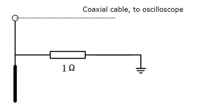
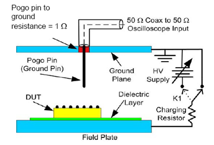
Equivalent circuit diagram
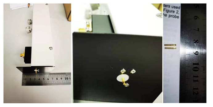
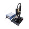
Test Probe Physical Reference Picture
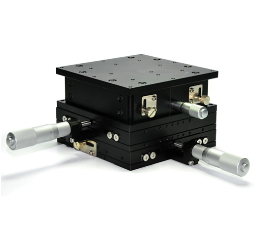
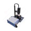
Base Physical Picture
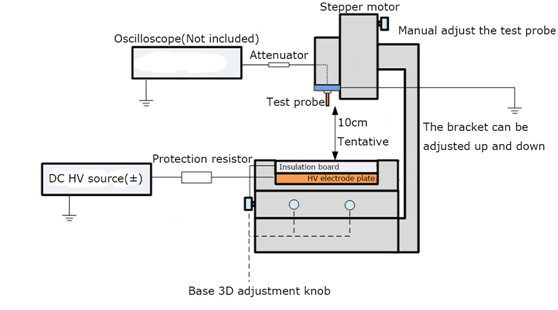
Schematic diagram of three-dimensional adjustment of the base (reference)
Test Operation Process:
1. Place the DUT on the insulation board, fix the fixture, and face the pin upward;
2. Manually adjust the three-dimensional knob of the base to make the pin of the DUT in the center;
3. Manually control the test probe to the maximum displacement, confirm that it is in contact with the pin, and then restore its position;
4. Set the probe movement speed to an appropriate value;
4. Start the high voltage source to XX volts to put the DUT in an electrostatically induced charged state;
5. Make the probe automatically move down quickly and contact the pin to complete the CDM discharge process. At the same time, the discharge waveform data is transmitted to the oscilloscope via a coaxial cable for display and storage.
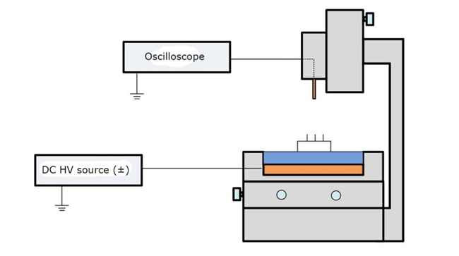
Schematic Diagram Of The Test Operation Process

 中文简体
中文简体