LM-79 Moving Detector Goniophotometer (Mirror Type C)
LSG-6000
High Precision Rotation Luminaire Goniophotometer
LSG-1890B
High Precision Rotation Luminaire Goniospectroradiometer
LSG-1890BCCD

Goniophotometer for Automotive and Signal Lamps
LSG-1950
Goniophotometer for Traffic Signal Lamps
LSG-1950S
VAD Fire Alarm Visual Alert Device Goniophotometer
LSG-1930
Compact Goniophotometer
LSG-1200A
LED Goniophotometer
LSG-1100
 LEDs and Luminaire Test Solutions
 LM-79 and LM-80 Test Solutions
 LED Driver Test Solutions
 Household Appliances Test Solutions
 Mobile and Network Test Solutions
 Automotive Electronics Test Solutions
 Audio-Video and IT Test Solutions
 Cable and Wire Test Solutions
 Plugs and Sockets Test Solutions
 Power Switch Test Solutions
 Transformer Test Solutions
 Electric Toys Test Solutions
 Energy Meter Test Solutions
 Motor-Operated Tool Test Solutions
Select an organization
to browse standards
Abstract
During the production, transportation and assembly of semiconductor chips, charged‑device‑model electrostatic discharge constitutes a major cause of unexpected failures of integrated circuits. Such failures feature strong concealment, ultra‑short pulse duration and high difficulty in failure reproduction. Conventional Human‑Body Model (HBM) and Machine Model (MM) tests cannot fully cover such failure risks. IC Component CDM ESD Testing Equipment reproduces the transient discharge phenomenon when charged devices contact grounded conductors and completes the evaluation of electrostatic tolerance for IC components. This paper takes LISUN ESD‑CDM CDM Semiconductor ESD Simulator as the research object. It discusses the working principle, hardware composition, standard compliance, complete test procedures and engineering application value of IC Component CDM ESD Testing Equipment, so as to provide a complete and implementable test reference for reliability research, mass‑production quality inspection and international compliance certification of semiconductor devices.
During handling on production lines, packaging transit and automated assembly, semiconductor chips accumulate electrostatic charges via friction and electric‑field induction. When device pins come into contact with grounded fixtures, PCB pads or metallic parts of automated equipment, nanosecond‑level transient discharge occurs, namely CDM charged‑device‑mode electrostatic discharge. The discharge pulse usually lasts less than 1 ns with peak current up to tens of amperes. Although the overall discharge energy is low, its power density is extremely high, which may directly break down the gate oxide layer of chips and result in burnt internal circuits, parameter drift or permanent functional failure. Many chips function properly after factory inspection yet suffer unexplained faults after circulation and assembly. A large proportion of such issues stem from latent damage induced by CDM electrostatic shocks, which can hardly be detected through conventional visual inspection.
Most traditional ESD test devices focus on the Human‑Body Model and Machine Model. Their device architecture and waveform acquisition capacity fail to satisfy stringent CDM test requirements, and they commonly suffer drawbacks such as cumbersome operation procedures, insufficient discharge waveform stability and large voltage control error. IC Component CDM ESD Testing Equipment is specially developed for charged‑device contact discharge scenarios. Adopting an integrated design of charge injection and contact discharge, it can precisely control charging voltage and discharge contact speed, fully capture transient current waveforms, quantify the CDM electrostatic shock tolerance limit of chips, identify device design defects in advance and reduce failure probability in subsequent mass production and application stages.
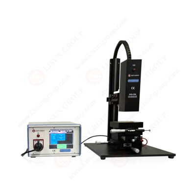
The complete LISUN ESD‑CDM CDM Semiconductor ESD Simulator system consists of three core units: high‑voltage DC power supply, test mainframe and electrostatic test probe. The equipment can independently perform CDM‑mode tests. It can also share the mainframe with the ESD‑883D Semiconductor ESD Simulator to expand composite tests covering CDM, HBM and MM models and satisfy multi‑dimensional evaluation of device electrostatic susceptibility. The high‑voltage DC power supply outputs controllable positive and negative high voltage to complete field‑induced charging of devices under test. The test mainframe holds the IC under test and is equipped with 3‑dimensional displacement adjustment and high‑voltage insulation protection structure. The electrostatic test probe performs contact discharge and integrates an attenuator to output discharge current waveform signals for external oscilloscope recording and analysis. Key hardware parameters of the equipment are summarized in the table below.
| Functional Unit | Item | Specification |
|---|---|---|
| High‑voltage DC Power Supply | Voltage Output Range | ±(50V~6kV) |
| High‑voltage DC Power Supply | Voltage Output Accuracy | ±(3% of reading +10V) |
| Test Mainframe | X/Y/Z 3‑axis Adjustment Range | 0‑10cm, adjustment resolution 0.1mm |
| Test Mainframe | Induction Plate Dimension | 12cm*12cm*2mm |
| Test Mainframe | Isolation Plate Dimension & Material | 12cm*12cm*0.4mm, FR4 insulation material |
| Electrostatic Test Probe | Maximum Current Measuring Capacity | ≥20A |
| Electrostatic Test Probe | Probe Moving Speed | 0.1cm/s‑5cm/s (program‑controlled & manual dual mode) |
| Electrostatic Test Probe | Standard Ground Plate Dimension | 63.5mm*63.5mm*6.35mm |
High‑voltage isolation protection is embedded inside the test mainframe. The high‑voltage induction plate is insulated to avoid safety risks caused by high‑voltage leakage and guarantee operator safety. The high‑voltage induction plate together with the FR4 isolation plate forms the test carrier platform. FR4 material meets JEDEC requirements for CDM test platform materials and generates uniform and stable electrostatic induction fields to ensure even charge distribution on devices during charging. The electrostatic test probe has a physical diameter of Φ1.5 mm and a telescopic travel of approximately 3 mm, compatible with mainstream semiconductor packages including DIP, SOP, QFP, BGA and TO. Equipped with a dedicated attenuator, the probe reserves signal acquisition interfaces for direct oscilloscope connection to capture nanosecond‑level discharge pulse waveforms. The device is fitted with a Chinese‑English Android touch screen for one‑click parameter configuration. Test data such as test voltage and current waveforms can be stored directly to improve test repeatability and efficiency.
LISUN ESD‑CDM, the IC Component CDM ESD Testing Equipment, is fully compliant with major domestic and international CDM electrostatic discharge test standards. International standards include ANSI/ESDA/JEDEC JS‑002‑2014, IEC 60749‑28:2022, AEC‑Q100‑011, EIA/JESD22‑C101 and JEITA ED‑4701/300 Test Method 305. The corresponding domestic standard is GB/T 4937.28‑2024 Semiconductor devices‑Mechanical and climatic test methods‑Part 28: Electrostatic discharge sensitivity tests‑Charged‑device model, which is identically converted from IEC 60749‑28:2022. For automotive‑grade chips, consumer‑grade integrated circuits and power semiconductors, this IC Component CDM ESD Testing Equipment can be used for component‑level CDM electrostatic susceptibility classification, reliability verification and third‑party certification tests, and generated test data can be directly adopted in certification reports.
Formal CDM testing on IC components shall strictly follow standard specifications to control key conditions such as positioning accuracy, charging settling time and probe moving speed and minimize test errors induced by manual operation. Step one is IC device mounting. Place the semiconductor device under test on the isolation plate and fix it with compatible fixtures with pins facing upward. Confirm no looseness or offset to avoid disturbance of discharge effects caused by device displacement during testing. Step two is position calibration. Adjust X/Y/Z 3‑axis knobs of the base to align the target pin right below the center of the test probe, with positioning calibration accuracy controlled within 0.1 mm to satisfy JEDEC positioning error requirements. Step three is probe commissioning. Move the probe manually to maximum travel and lower it slowly until it just touches the device pin. Excessive pressing that causes physical chip damage shall be strictly avoided. After contact confirmation, retract the probe to standby position and reserve a 5‑10 mm safety gap between probe and pin. Step four is parameter preset. Set vertical probe moving speed on the touch interface. For chips with fragile packages, 0.5‑2 cm/s is recommended to prevent mechanical damage from the probe. Step five is electrostatic charging. Set target voltage on the high‑voltage power supply and perform field‑induced charging on the device via the high‑voltage induction plate. Maintain a settling time of 1‑2 seconds to achieve full and even charge distribution inside the device. Step six is discharge test execution. Start the automatic probe downward movement routine. The probe contacts the device pin to trigger CDM discharge. Instant discharge current signals are transmitted via the attenuator to the oscilloscope with sampling rate no lower than 1 GHz for nanosecond‑level pulse waveform capture and saving. After single‑polarity discharge on one pin, switch high‑voltage polarity and target pin to perform cyclic positive‑and‑negative CDM discharge stress tests on all pins. Upon test completion, compare electrical parameters and functional status of the device before and after stress to determine its CDM electrostatic susceptibility rating.
IC Component CDM ESD Testing Equipment delivers multiple values across the semiconductor industrial chain. At the chip research and development stage, design engineers can utilize this equipment to locate CDM‑sensitive weak points inside chips and optimize on‑chip ESD protection circuit design. At packaging houses, it can be applied for incoming inspection and finished‑product reliability screening to eliminate products with insufficient CDM tolerance in advance. For automotive‑grade chips requiring compliance certification, test outputs support certification items such as AEC‑Q100. It should be noted that CDM discharge pulses are picosecond‑to‑nanosecond high‑speed signals. Cables, attenuators and oscilloscope bandwidth of the whole test system directly affect waveform fidelity. In practical testing, regular system calibration shall be performed to guarantee that voltage error and current waveform indexes meet standard requirements. Devices with larger package sizes require extended charging settling time for sufficient charge accumulation.
As semiconductor process nodes keep shrinking, gate oxide layers of chips become thinner and integrated circuits grow more vulnerable to CDM electrostatic shocks. CDM has become a major contributor to chip failures. IC Component CDM ESD Testing Equipment can realistically reproduce charged‑device contact discharge scenarios in production and assembly and realize high‑precision, high‑repeatability component‑level CDM electrostatic susceptibility testing. LISUN ESD‑CDM CDM Semiconductor ESD Simulator overcomes shortcomings of conventional CDM test instruments. Its hardware structure, control accuracy and standard compliance can satisfy practical demands for research, quality inspection and certification in the domestic semiconductor industry. When conducting reliability verification for integrated circuits, enterprises shall attach importance to CDM testing and incorporate IC Component CDM ESD Testing Equipment into reliability test systems. Latent failures induced by CDM static electricity can be avoided at component level and overall reliability of integrated circuit products can be improved.
Tags:ESD-CDMYour email address will not be published. Required fields are marked *

 English
 中文简体
中文简体 English
 Русский
 Español
 Português
 Türkçe
 العربية
 Deutsch
 Polski
 Italiano
 Français
 한국어
한국어 ไทย
ไทย Tiếng Việt
 日本語
日本語