LM-79 Moving Detector Goniophotometer (Mirror Type C)
LSG-6000
High Precision Rotation Luminaire Goniophotometer
LSG-1890B
High Precision Rotation Luminaire Goniospectroradiometer
LSG-1890BCCD

Goniophotometer for Automotive and Signal Lamps
LSG-1950
Goniophotometer for Traffic Signal Lamps
LSG-1950S
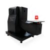
VAD Fire Alarm Visual Alert Device Goniophotometer
LSG-1930
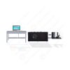
Compact Goniophotometer
LSG-1200A
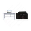
LED Goniophotometer
LSG-1100
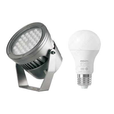 LEDs and Luminaire Test Solutions
 LM-79 and LM-80 Test Solutions
 LED Driver Test Solutions
 Household Appliances Test Solutions
 Mobile and Network Test Solutions
 Automotive Electronics Test Solutions
 Audio-Video and IT Test Solutions
 Cable and Wire Test Solutions
 Plugs and Sockets Test Solutions
 Power Switch Test Solutions
 Transformer Test Solutions
 Electric Toys Test Solutions
 Energy Meter Test Solutions
 Motor-Operated Tool Test Solutions
Select an organization
to browse standards
Throughout the full workflow of semiconductor device R&D, packaging, manufacturing, transportation and assembly, electrostatic discharge represents a major cause of latent chip failures. Electrostatic pulses can be generated by human contact, automated equipment contact and material friction. Even without visible discharge phenomena, irreversible damage may occur to chip gate oxide layers and PN junctions. Such damage rarely leads to immediate complete device failure; instead, latent defects are formed which trigger random functional faults during later installation and end‑user operation, bringing substantial quality risks to finished products. To evaluate electrostatic withstand capability before component delivery, the HBM/MM ESD Simulator for IC has become indispensable test equipment in semiconductor reliability laboratories. This paper focuses on LISUN ESD‑883D HBM/MM semiconductor ESD generator, illustrating the working principle, hardware features, standard compliance and industrial application scenarios of the HBM/MM ESD Simulator for IC.
Basic Principle and Equipment Positioning of HBM/MM ESD Simulator for IC
The ESD‑883D semiconductor electrostatic discharge generator is a high‑precision ESD immunity test device designed by LISUN specifically for semiconductor components such as chips, diodes, transistors and IC modules. Its core function is to simulate two common ESD models occurring during semiconductor production, transportation and assembly: Human‑Body Model (HBM) and Machine Model (MM). Through standardized high‑voltage pulse injection, it assesses the electrostatic shock withstand limit of semiconductor devices, detects latent failures including gate breakdown and PN‑junction damage caused by electrostatic stress in advance, and provides critical test evidence for reliability design and outgoing quality inspection of semiconductor components. As a mainstream HBM/MM ESD Simulator for IC, this instrument differs from system‑level ESD generators complying with IEC 61000‑4‑2 for finished‑product testing. It is dedicated to component‑level chip stress testing and strictly reproduces discharge waveforms defined by JEDEC, IEC and MIL‑STD‑883 standards.
The HBM model simulates electrostatic discharge when a charged human finger touches chip pins, replicating real‑world conditions where operators handle components inside manufacturing workshops. The MM model simulates discharge from charged metallic automated equipment such as pick‑and‑place machines and probe stations contacting chips. The MM discharge loop has almost no series resistance and delivers higher peak discharge current, producing more destructive effects on semiconductor devices. The HBM/MM ESD Simulator for IC reproduces equivalent circuits of both models via internal capacitance‑resistance networks. High‑voltage pulses of graded levels are applied to pins of the device under test. Electrical performance measurements after stress help judge whether device damage has occurred, determine component ESD sensitivity levels, and supply test data for iterative optimization of on‑chip ESD protection circuits.

ESD-883D Electrostatic Discharge (ESD) IC Tester
Hardware Configuration and Key Technical Specifications of ESD‑883D HBM/MM ESD Simulator for IC
Adopting modular circuit architecture, the ESD‑883D supports one‑click switching between HBM and MM test modes and integrates a high‑precision voltage feedback system with discharge voltage error within ±3%. The dust‑proof and corrosion‑resistant enclosure allows deployment in Class 1000 semiconductor clean‑room environments. A bilingual Chinese‑English Android touch screen serves as human‑machine interface, enabling presetting of standard test levels such as HBM 2 kV, 4 kV and 8 kV. Compatible tooling includes TO‑package fixtures and SMD test jigs, covering semiconductor devices with DIP, SOP, QFP and other package types without frequent fixture replacement. Key technical specifications are listed in the table below.
| Parameter Item | Human‑Body Model (HBM) | Machine Model (MM) |
|---|---|---|
| Output Voltage Range | 0.1~8kV, accuracy ±5% | 100~800V, accuracy ±5% |
| Output Polarity | Positive, Negative, Alternating positive‑negative | Positive, Negative, Alternating positive‑negative |
| Trigger Mode | Single shot, counter mode, internal auto‑trigger | Single shot, counter mode, internal auto‑trigger |
| Discharge Capacitance | 100pF±10% | 200pF±10% |
| Discharge Resistance | 1500Ω±10% | 0Ω±10% |
| Discharge Interval & Count | 1‑99 s interval, 1‑999 shots | 1‑99 s interval, 1‑999 shots |
| System Power Supply | AC 100‑240V, 50/60Hz, 300W | |
This HBM/MM ESD Simulator for IC features expandability. An optional ESD‑CDM module can upgrade the platform to support HBM / MM / CDM three‑in‑one testing, covering three mainstream component‑level ESD models to satisfy stringent semiconductor reliability validation requirements. Hardware circuit parameters fully comply with HBM and MM circuit requirements defined by GB/T 4937.26‑2023, GB/T 4937.27‑2023, IEC 60749‑26, IEC 60749‑27, ANSI/ESDA/JEDEC JS‑001‑2024 and AEC‑Q100, ensuring waveform compliance and enabling test data submission for product certification.
Test Procedure and Failure‑Criteria Logic for HBM/MM ESD Simulator for IC
When performing HBM and MM tests with the ESD‑883D, the semiconductor device under test shall be mounted on dedicated fixtures, and pin connections shall be completed in accordance with standard requirements. Test conditions including discharge voltage, polarity, shot count and discharge interval are configured. Testing generally adopts a step‑up voltage strategy: electrostatic pulses are applied with gradually increased voltage levels. DC parametric tests and functional verification are executed after each stress sequence. Increased leakage current, functional disorder or communication failure indicates that the device has reached its electrostatic withstand limit.
Chip failures are classified into catastrophic failure and latent failure. Catastrophic failure manifests as direct open‑circuit or short‑circuit with fully abnormal electrical parameters. Latent failure presents as parametric drift while the device remains operational, yet reliability is severely degraded and total breakdown may occur under subsequent stress such as temperature cycling or vibration. The value of the HBM/MM ESD Simulator for IC lies in exposing latent defects originating from R&D and manufacturing through standardized electrostatic stress. During R&D, test results guide optimization of on‑chip ESD protection diodes and clamping circuits. Packaging houses utilize sampling tests to evaluate whether packaging and wire‑bonding processes degrade component ESD immunity performance.
Practical Application Value of ESD‑883D across the Semiconductor Industry Chain
At the chip‑design R&D stage, the HBM/MM ESD Simulator for IC is used for reliability validation of MCUs, power‑management ICs, RF chips as well as SiC and GaN wide‑bandgap devices. Design engineers leverage HBM and MM testing to verify protection‑circuit performance, define component ESD sensitivity levels, and optimize chip layout and protection‑device parameters, avoiding costly redesign caused by insufficient ESD robustness after tape‑out.
Within semiconductor packaging factories, the ESD‑883D supports outgoing sampling inspection for packaged components covering DIP, SOP, QFP and other packages. Mass sampling monitors device‑performance degradation induced by manufacturing‑process variation and guarantees conformance with JEDEC specifications for shipped products. Automotive semiconductors face strict electrostatic‑reliability requirements. Vehicle‑grade MCUs, millimeter‑wave radar chips and IGBT gate‑driver ICs must complete HBM and MM testing according to AEC‑Q100. The HBM/MM ESD Simulator for IC reproduces electrostatic shocks occurring during assembly and mitigates safety hazards such as instrument‑cluster blackouts and ADAS signal misreporting triggered by electrostatic damage to on‑board systems. Military and aerospace chips also rely on this equipment for rigorous ESD validation following MIL‑STD‑883 Method 3015 and GJB 548B‑2020.
Third‑party testing laboratories conduct compliance tests with the ESD‑883D and deliver CNAS‑traceable test reports supporting CE, UL and other international market‑access certifications. Periodic instrument calibration satisfies instrument requirements for ISO 17025 laboratory accreditation and underpins laboratory capability development. For consumer‑electronics applications, SoCs, Bluetooth chips and smart‑home MCUs also undergo ESD‑sensitivity evaluation on the HBM/MM ESD Simulator for IC to reduce after‑sales failure rates such as system crash and hardware damage in end products.
Conclusion
Electro‑static damage represents a non‑negligible reliability risk for semiconductor devices. Many early‑stage chip failures originate from electrostatic stress encountered during design, packaging and assembly. Represented by the ESD‑883D, the HBM/MM ESD Simulator for IC fully realizes component‑level HBM and MM electrostatic‑discharge simulation and complies with global semiconductor ESD test standards. It covers the full workflow of chip design, packaging, automotive‑grade and military‑spec validation and third‑party certification. Standardized stress testing using the HBM/MM ESD Simulator for IC identifies ESD weak points in advance, optimizes protection schemes and screens defective components, lowering end‑product failure probability from the source and delivering solid test assurance for mass production and market deployment of semiconductor devices. Driven by rapid growth of wide‑bandgap semiconductors and automotive chips, demand for component‑level ESD testing keeps rising, making the HBM/MM ESD Simulator for IC core infrastructure within semiconductor‑reliability laboratories.
Your email address will not be published. Required fields are marked *

 English
 中文简体
中文简体 English
 Русский
 Español
 Português
 Türkçe
 العربية
 Deutsch
 Polski
 Italiano
 Français
 한국어
한국어 ไทย
ไทย Tiếng Việt
 日本語
日本語