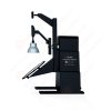
LM-79 Moving Detector Goniophotometer (Mirror Type C)
LSG-6000
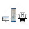
High Precision Rotation Luminaire Goniophotometer
LSG-1890B
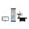
High Precision Rotation Luminaire Goniospectroradiometer
LSG-1890BCCD

Goniophotometer for Automotive and Signal Lamps
LSG-1950
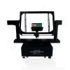
Goniophotometer for Traffic Signal Lamps
LSG-1950S
VAD Fire Alarm Visual Alert Device Goniophotometer
LSG-1930
Compact Goniophotometer
LSG-1200A
LED Goniophotometer
LSG-1100
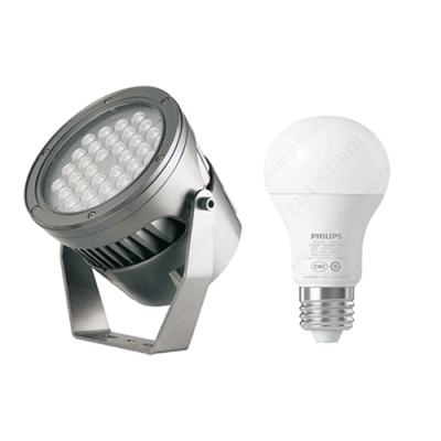 LEDs and Luminaire Test Solutions
 LM-79 and LM-80 Test Solutions
 LED Driver Test Solutions
 Household Appliances Test Solutions
 Mobile and Network Test Solutions
 Automotive Electronics Test Solutions
 Audio-Video and IT Test Solutions
 Cable and Wire Test Solutions
 Plugs and Sockets Test Solutions
 Power Switch Test Solutions
 Transformer Test Solutions
 Electric Toys Test Solutions
 Energy Meter Test Solutions
 Motor-Operated Tool Test Solutions
Select an organization
to browse standards
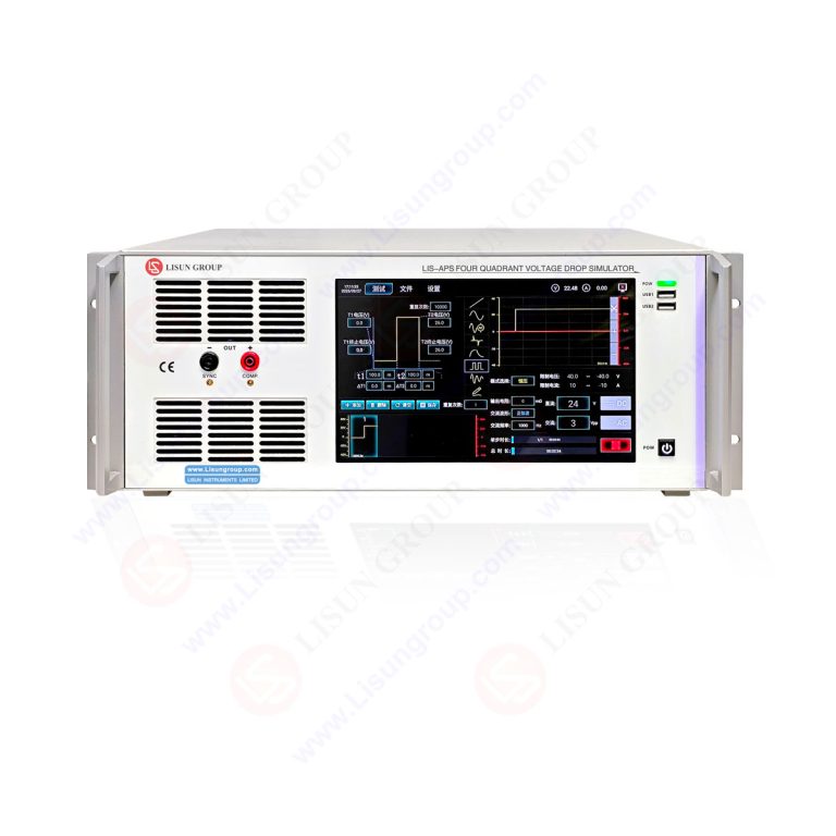
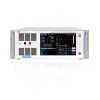
Product No: LIS-OFFSET-D20A
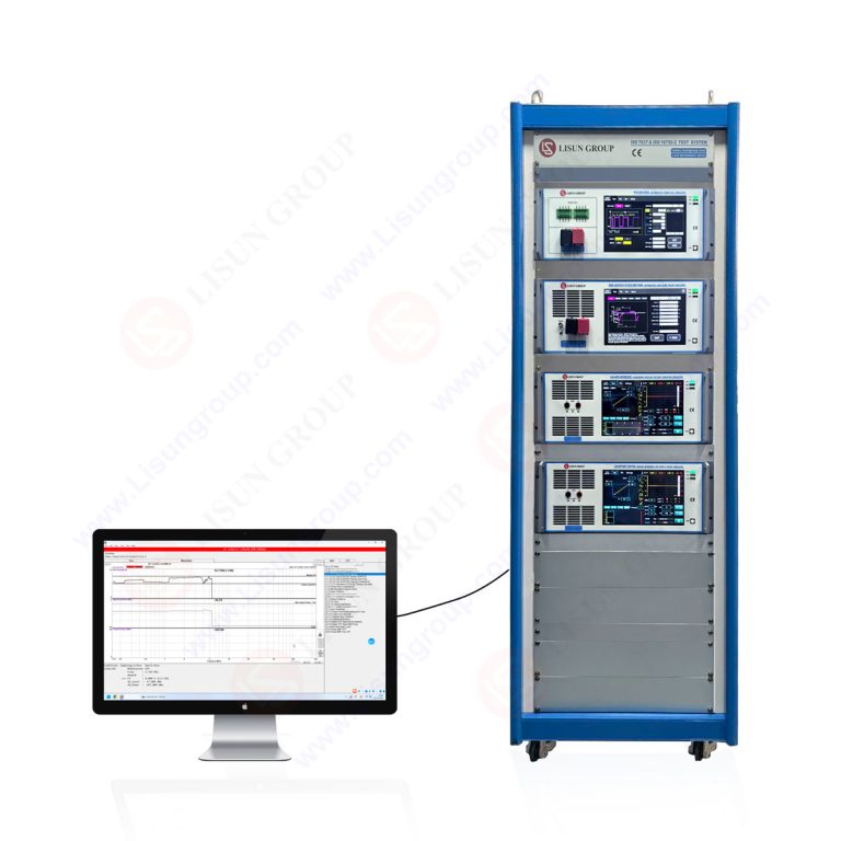
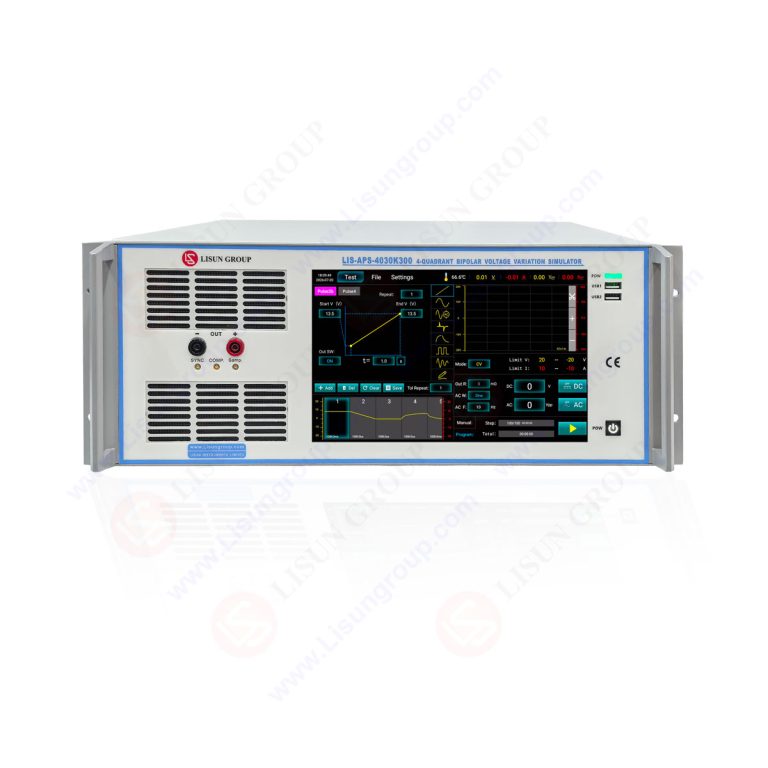
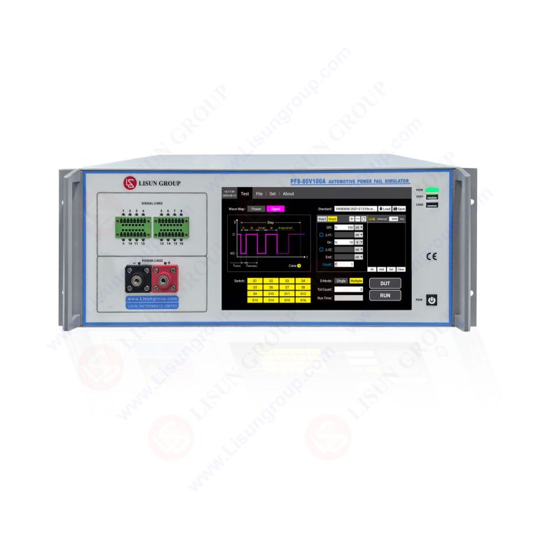
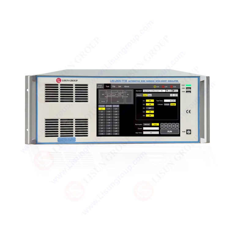
LIS-OFFSET-D20A Ground Reference and Power Offset Simulator is designed and developed in strict accordance with ISO 16750-2:2023 Clause 4.8. The equipment adopts a four-quadrant bipolar power supply architecture. This equipment is mainly used to simulate the multi-power supply circuit conditions of vehicles and verify the operational reliability of on-board electrical components in an environment with multiple power supplies and multiple groundings. It is widely compatible with the electrical systems of all types of road vehicles from major global automakers, including 12V, 24V, 36V and 48V, and is a dedicated device for automotive electronic and electrical reliability testing.
Standards:
| Standards No. | Standards Name |
| ISO 16750-2:2023 Clause 4.8 | Road vehicles — Environmental conditions and testing for electrical and electronic equipment — Part 2: Electrical loads |
| Ford EMC-CS-2009.1 Clause 18.0 | Electromagnetic Compatibility Specification for Automotive Electrical & Electronic Components |
| BMW GS 95024 Section 5.1 | Electrical and Electronic Components in Motor Vehicles – Requirements and Tests |
| Nissan 28400 | Automotive Electrical and Electronic Component Test Specification |
| FMC1278 CI 210 | Automotive Electrical & Electronic Test Standard |
| GMW3097 | General Motors EMC Basic Specification |
| GB/T 28046.2-2019 | 道路车辆 电气及电子设备的环境条件和试验 第 2 部分:电气负荷 |
Specifications:
| LISUN Model | LIS-OFFSET-10V10A | LIS-OFFSET-D20A | LIS-OFFSET-D50A | LIS-OFFSET-D100A | LIS-OFFSET-D200A |
| Voltage Range | 0~±5V | ||||
| Current Range | 0~10A | 0~20A | 0~50A | 0~100A | 0~200A |
| Number of Channels | Single Channel (requires use with LIS-APS-4030K300) | Built-in the independent dual-channels programmable power supplies (Can be tested individually) | |||
| Voltage Accuracy | 0.1% FS(±5~±10 mV) | ||||
| Current Accuracy | 0.5% FS(±10~±30 mA) | ||||
| Setting Accuracy | Min. 1 mV | ||||
| Output Voltage Frequency | DC~100 KHz | ||||
| Voltage Rise Rate | ≥5 V/µS | ||||
| Frequency Output Method | Fixed, linear, logarithmic | ||||
| Transient Current | Three times the continuous current, with a duration of 10~200ms. | ||||
| Combined Waveform Editing | linear | ||||
| Editable Steps of Combined Waves | Maximum 255 steps | ||||
| Min Editable Time for Combined Waves | 100 µS | ||||
| Protection Function | It has overcurrent, overvoltage, short circuit and overtemperature protection. | ||||
| Control System | 10.1-inch Chinese/English Android capacitive touchscreen display + supports remote control via PC software | ||||
| Interface | LAN、USB、RS485 | ||||
| Working Power Supply | AC110~250V,50Hz/60Hz | ||||
| Calibration Certificate | Please click: ISO 17025 CNAS Third-Party Calibration Certifiate | ||||
Working Principle:
The equipment is equipped with two independent programmable power supplies, which can apply independent offset voltages to the power and ground pins of the device under test (DUT). Uoffset1 is the power line offset voltage, and Uoffset2 is the ground offset voltage; U1/U2 are the power supply lines for the DUT, and GND1/GND2 are the ground lines for the DUT.
The power and ground offset voltages can be flexibly configured according to standards to replicate the potential difference conditions in a real vehicle. If multiple ground pins inside the DUT are interconnected, the ground offset voltage will act synchronously on all ground terminals, realistically simulating the automotive electrical environment and completing product reliability testing.
| Test Sequence Number | Description of Test Conditions | Reference Voltage (VS) | Power Supply Offset (Voffset1) | Ground Offset (Voffset2) |
| 1 | 1V GND Offset and no US offset | UB+(UA-UB)/2 | 0 V | 1 V |
| 2 | 1V GND Offset and 1V US offset | UB+(UA-UB)/2 | 1 V | 1 V |
| 3 | 1V GND Offset and -1V US offset | UB+(UA-UB)/2 | -1 V | 1 V |
| 4 | -1V GND Offset and no US offset | UB+(UA-UB)/2 | 0 V | -1 V |
| 5 | -1V GND Offset and 1V US offset | UB+(UA-UB)/2 | 1 V | -1 V |
| 6 | -1V GND Offset and -1V US offset | UB+(UA-UB)/2 | -1 V | -1 V |
| 7 | No GND Offset and 1V US offset | UB+(UA-UB)/2 | 1 V | 0 V |
| 8 | No GND Offset and -1V US offset | UB+(UA-UB)/2 | -1 V | 0 V |

 English
 中文简体
中文简体 English
 Русский
 Español
 Português
 Türkçe
 العربية
 Deutsch
 Polski
 Italiano
 Français
 한국어
한국어 ไทย
ไทย Tiếng Việt
 日本語
日本語